Semiconductor memory device and method of manufacturing the same
Inactive Publication Date: 2002-08-22
TOSHIBA MEMORY CORP
View PDF1 Cites 222 Cited by
Summary
Abstract
Description
Claims
Application Information
AI Technical Summary
This helps you quickly interpret patents by identifying the three key elements:
Problems solved by technology
Method used
Benefits of technology
Problems solved by technology
When the thickness of the capacitor insulating film is reduced, a tunnel current flows and hence insulation properties can not be maintained.
Consequently, an etching limit to a silicon substrate in the case of a trench cell, and boring of a contact hole to bring a lower portion of a capacitor structure into contact with an upper portion thereof, filling of a conductor in this contact hole, and uniform covering properties of a dielectric in the case of a stacked cell come into question, and hence it has been said that those structures are unfit for further scale-down to a size under 100 nm.
In any case, in these gain cells, the number of devices is two or more, and gates (word lines) and drains (bit lines) are not common but separate for a write operation and a read operation, whereby the number of connections is large, and consequently, these gain cells are unfit for scale-down.
Also, as for write speed, it is more unfavorable compared with ordinary SRAM and DRAM.
As for write speed, this gain cell is more unfavorable compared with ordinary SRAM and DRAM.
Moreover, it is necessary to write "0" before writing "1", and thus regarding write speed, it is more unfavorable than ordinary SRAM and DRAM.
Also in this gain cell, it is necessary to write "1" before writing "0", and regarding write speed, it is more unfavorable than ordinary SRAM and DRAM.
As described above, those recently proposed as a new DRAM need a special transistor structure and hence they have a complicated structure.
Alternatively, even if they have a relatively simple structure, they have a drawback in controllability, whereby the achievement of high integration and high performance is difficult.
Method used
Image
Click on the blue label to locate the original text in one second.
Reading with bidirectional positioning of images and text.
Examples
fifth embodiment
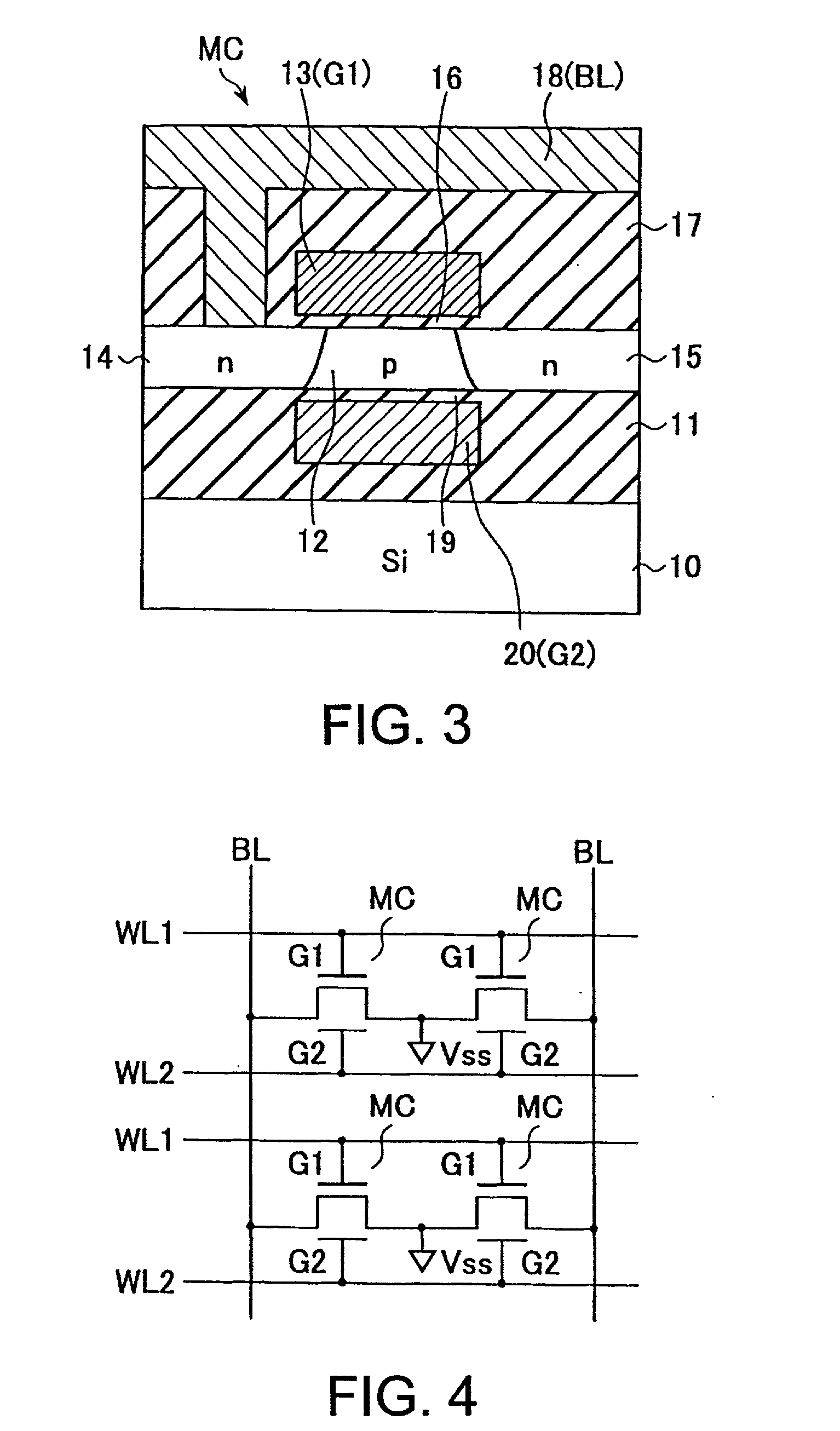
[0299] FIG. 11 shows the sectional structure of a DRAM cell according to a fifth embodiment. In this embodiment, a vertical MIS transistor is formed in a p-type pillar silicon portion 30 formed on the silicon substrate 10 instead of the SOI substrate. Specifically, the n-type drain region 14 is formed on the top of the pillar silicon portion 30 and the n-type source region 15 is formed at the bottom thereof. Moreover, the first gate (G1) 13 and the second gate (G2) 20 are formed to face each other on both side faces of the pillar silicon portion 30. Hence, the memory cell MC is composed of the vertical MIS transistor with the pillar silicon portion 30 as a floating channel body, instead of the SOI substrate.
[0300] This vertical MIS transistor structure is known as an SGT (Surrounding Gate Transistor).
[0301] Also by this embodiment, the same effect as that of the preceding embodiment can be obtained.
[0302] Next, manufacturing processes corresponding to the aforementioned respective e...
first embodiment
Manufacturing Process Corresponding to First Embodiment
[0303] FIG. 12 to FIG. 18 show the process of manufacturing a DRAM cell corresponding to the first embodiment shown in FIG. 3. In this embodiment, two silicon substrates are used in order that two gates 13 and 20 are disposed above and below the silicon layer. As shown in FIG. 12, in a first silicon substrate 101, trenches 102 are worked each as an alignment mark at the outside of a cell array region. As shown in FIG. 13, an oxide film 103 is buried in each of the trenches 102. The depth of the trench 102 is more than the thickness of an SOI layer which is adjusted by shaving the silicon substrate 101 later. More specifically, as will be described later, since the silicon substrate 101 becomes the silicon layer 12 in FIG. 3, the trenches 102 are formed more deeper than the thickness of the silicon layer 12.
[0304] Thereafter, as shown in FIG. 14, the second gates 20 (G2) are pattern-formed on the silicon substrate 101 with the ga...
second embodiment
Manufacturing Process Corresponding to Second Embodiment
[0307] FIG. 19 to FIG. 26 show the process of manufacturing a DRAM cell corresponding to the second embodiment shown in FIG. 8. Also in this embodiment, two silicon substrates are used in order that two gates 13 and 20 are disposed above and below the silicon layer. As shown in FIG. 19, in the first silicon substrate 101, the trenches 102 are worked each as an alignment mark at the outside of a cell array region. As shown in FIG. 20, the oxide film 103 is buried in each of the trenches 102. The depth of the trench 102 is more than the thickness of an SOI layer which is adjusted by shaving the silicon substrate 101 later. More specifically, as will be described later, since the silicon substrate 101 becomes the silicon layer 12 in FIG. 8, the trenches 102 are formed more deeper than the thickness of the silicon layer 12.
[0308] Thereafter, as shown in FIG. 21, the first gates 13 (G1) are pattern-formed on the silicon substrate 10...
PUM
Abstract
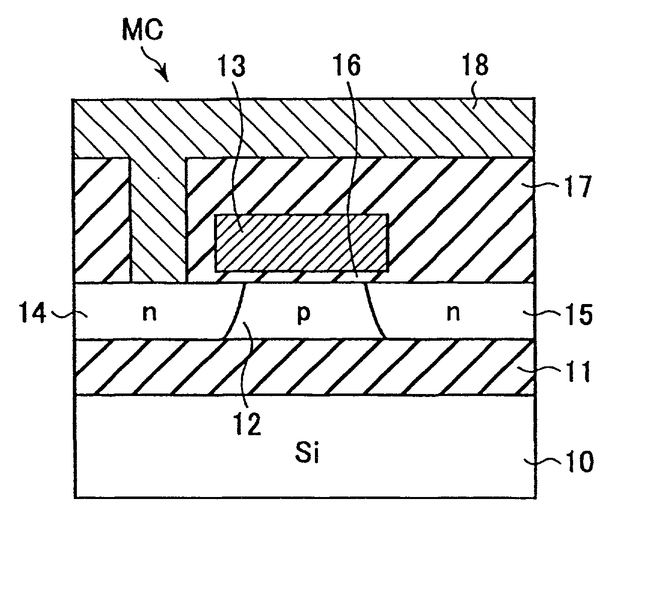
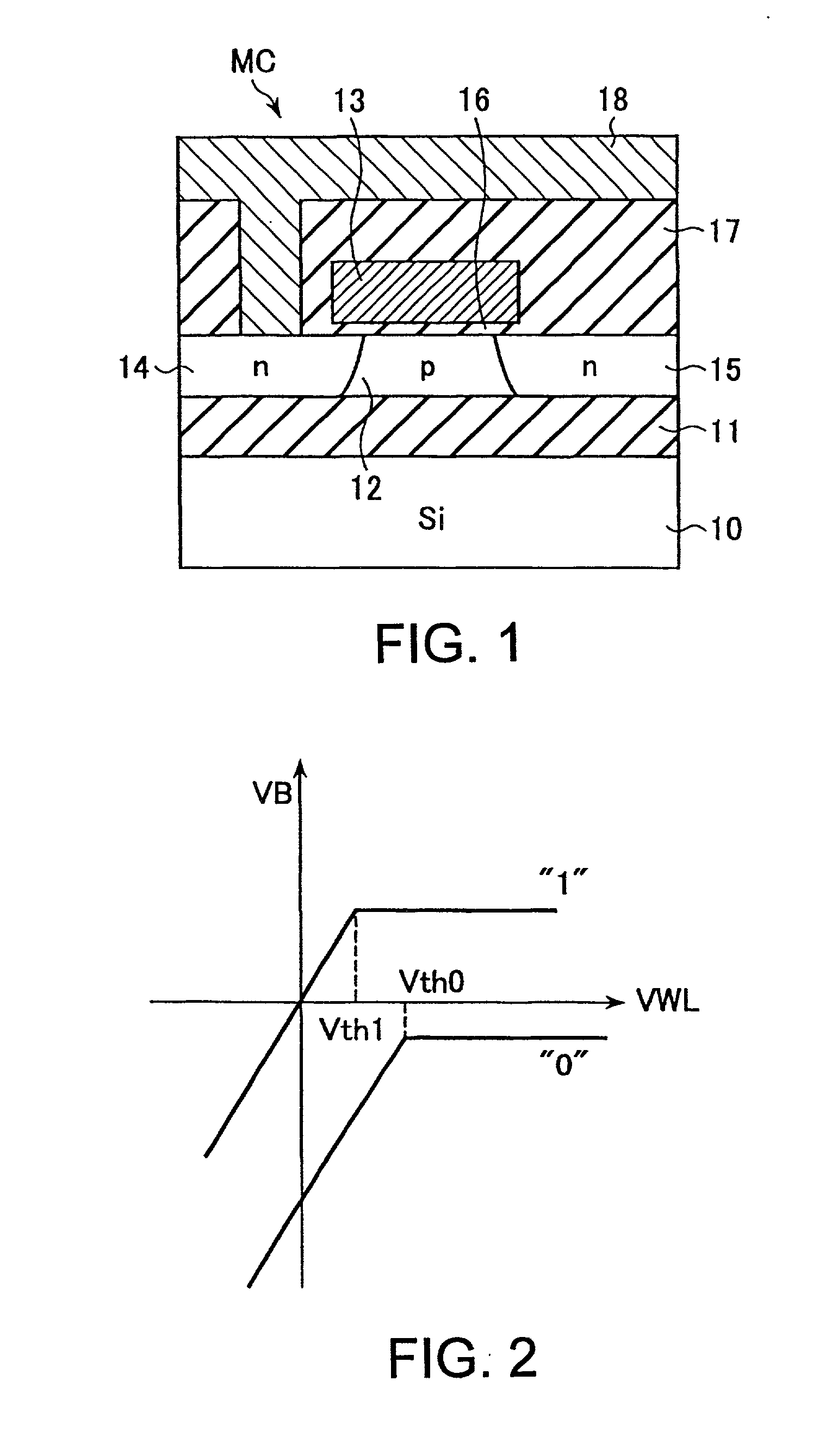
A semiconductor memory device having MIS transistors to constitute memory cells (MC), each of the MIS transistors including a semiconductor layer (12), a source region (15) formed in the semiconductor layer, a drain region (14) formed apart from the source region in the semiconductor layer, the semiconductor layer between the source region and the drain region serving as a channel body in a floating state, a main gate (13) provided between the source region and the drain region to form a channel in the channel body; and an auxiliary gate (20) provided separately from the main gate to control a potential of the channel body by capacitive coupling, the auxiliary gate being driven in synchronization with the main gate. The MIS transistor has a first data state in which the channel body is set at a first potential and a second data state in which the channel body is set at a second potential.
Description
[0001] This application claims the benefit of priority under 35 U.S.C. .sctn. 119 to Japanese Patent Application Nos. 2001-41828, 2001-191781 and 2001-328204 filed on Feb. 19, 2001, Jun. 25, 2001 and Oct. 25, 2001, respectively, the entire contents of which are incorporated by reference herein.[0002] 1. Field of the Invention[0003] The present invention relates to a semiconductor memory device which dynamically stores data with a channel body as a storage node.[0004] 2. Description of the Related Art[0005] A memory cell of a DRAM generally used as a large capacity RAM is composed of one MOS transistor and one capacitor, and electric charge is stored in the capacitor with using the MOS transistor as a selection switch. Data is read out at the sight of a change in the potential of a bit line by redistributing the electric charge stored in the cellcapacitor to the electric charge of the bit line. Accordingly, there is a lower limit to the storage charge amount of the cell capacitor re...
Claims
Application Information
Patent Timeline
Application Date:The date an application was filed.
Publication Date:The date a patent or application was officially published.
First Publication Date:The earliest publication date of a patent with the same application number.
Issue Date:Publication date of the patent grant document.
PCT Entry Date:The Entry date of PCT National Phase.
Estimated Expiry Date:The statutory expiry date of a patent right according to the Patent Law, and it is the longest term of protection that the patent right can achieve without the termination of the patent right due to other reasons(Term extension factor has been taken into account ).
Invalid Date:Actual expiry date is based on effective date or publication date of legal transaction data of invalid patent.

