

Method of forming an insulating layer in a trench isolation type semiconductor device
- Summary
- Abstract
- Description
- Claims
- Application Information
AI Technical Summary
Benefits of technology
Problems solved by technology
Method used
Image

Examples
Embodiment Construction
[0020] Korean Patent Application No. 2001-11142, filed on Mar. 5, 2001, and entitled: "Method of Forming Insulating Layer in Trench Isolation Type Semiconductor Device," is incorporated herein by reference in its entirety.
[0021] The present invention now will be described more fully with reference to the accompanying drawings, in which preferred embodiments of the invention are shown. This invention may, however, be embodied in many different forms and should not be construed as being limited to the embodiments set forth herein; rather, these embodiments are provided so that this disclosure will be thorough and complete, and will fully convey the concept of the invention to those skilled in the art.
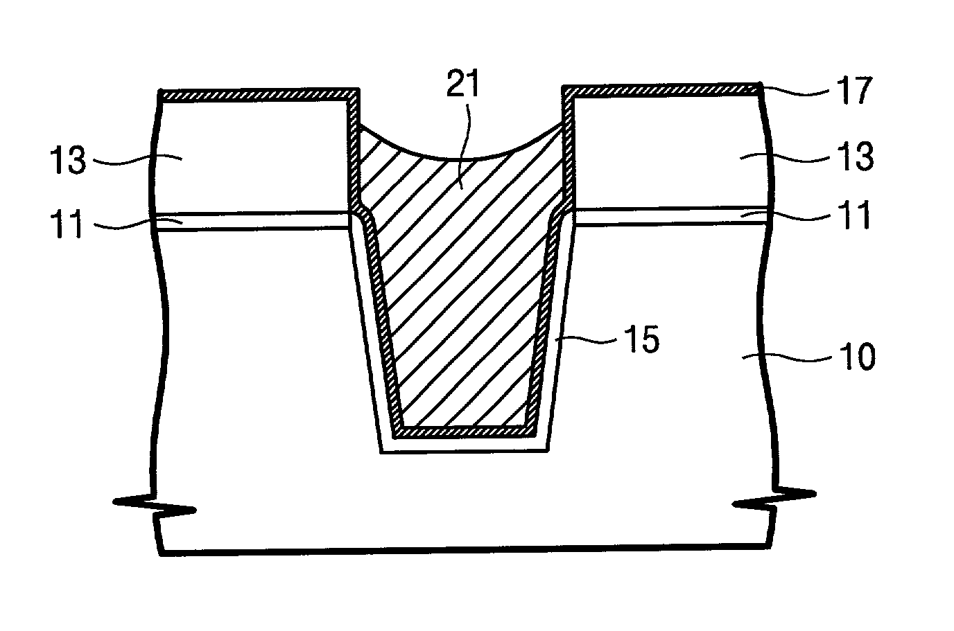
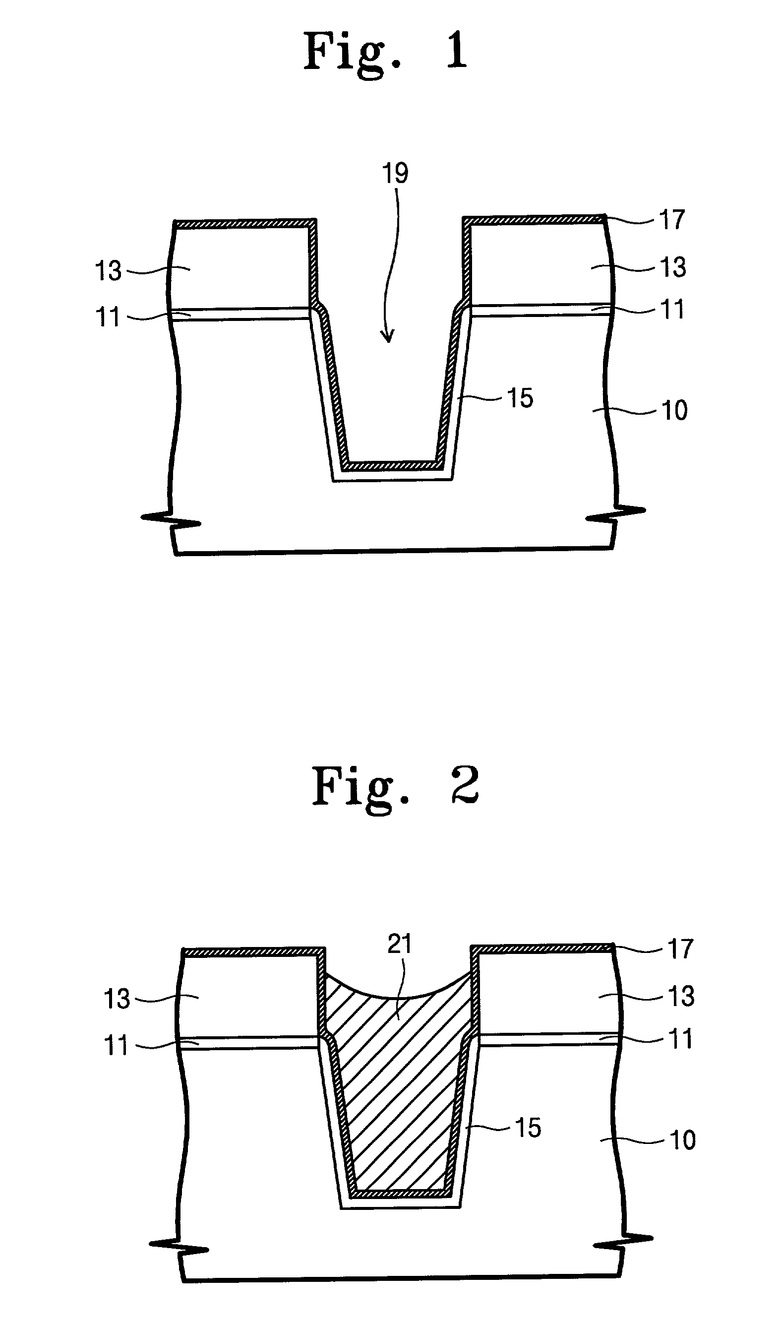
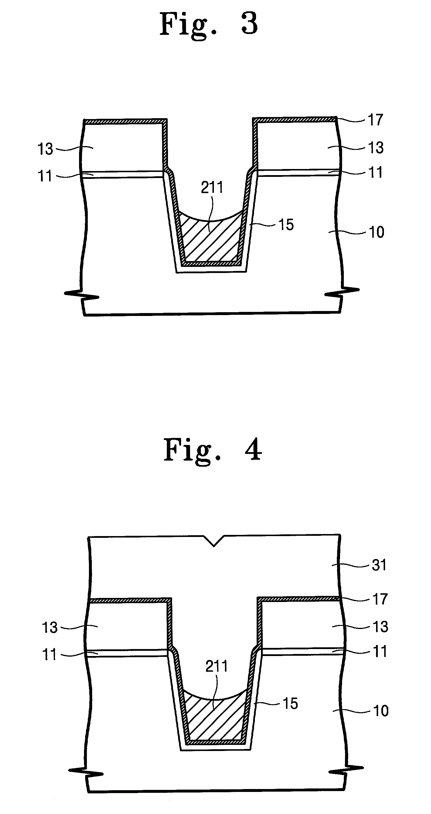
[0022] Referring to FIG. 1, a silicon nitride layer (not indicated) is stacked on a semiconductor substrate 10 on which a pad oxide layer 11 is formed. Using a photoresist (not shown), the silicon nitride layer is patterned to form a trench etch mask pattern 13 through exposure and etch s...
PUM
 Abstract
Description
Claims
Application Information