Overlay alignment metrology using diffraction gratings

a technology of overlay and alignment metrology, which is applied in semiconductor/solid-state device testing/measurement, semiconductor/solid-state device details, instruments, etc., can solve the problems of not necessarily solving the lines of the grating, and achieve the effects of reducing the dependence of measurements, limiting the space available for vibration damping, and measuring overlay errors

Inactive Publication Date: 2002-10-31
TOKYO ELECTRON LTD
View PDF28 Cites 266 Cited by
  • Summary
  • Abstract
  • Description
  • Claims
  • Application Information

AI Technical Summary

Benefits of technology

0035] It is another object of the present invention to measure overlay error with an optical instrument integrated into a process tool. This method and apparatus overcomes the difficulties associated with vibrations caused by the process tool and the limited space available for vibration damping. The apparatus comprises a process tool with at least one process chamber and a sample handler, an optical system in operative communication with the process tool, a computer equipped with an inverse model for interaction of light between two gratings where at least one parameter of the model is a lateral offset between two gratings.
0036] It is another object of the present invention to measure the overlay error by comparing the optical characteristics of grating pairs with substantially different perfect-overlay offsets. This reduces the dependence of the measurements on ancillary properties of the sample. It also reduces the burden on inverse scattering calculations.
0037] It is another aspect of the present invention to increase the range of unambiguous overlay error measurement from overlaying gratings. One approach is to offset symmetric gratings by one fourth of the grating pitch when the overlay error is zero, so that positive and negative overlay errors have the least ambiguity, regardless of the optical system. Another approach to extend the range of unambiguously detectable overlay errors is to make at least one of the gratings in the pair substantially asymmetric, that is to have the unit cell of its pattern asymmetric. Another approach is to combine a scatterometry measurement of offset with an imaging measurement of offset (similar to the prior art, e.g., using box-in-box). A fourth approach is to have grating pairs with different pitches, preferably in a substantially irrational ratio, to measure the same component of overlay error. These four approaches may be used either separately or in combination to extend the range of unambiguously detectable overlay errors.

Problems solved by technology

The spot of the optical instrument preferably covers many periods of the gratings and it does not necessarily resolve the lines of the grating.

Method used


Image

  • Overlay alignment metrology using diffraction gratings
  • Overlay alignment metrology using diffraction gratings
  • Overlay alignment metrology using diffraction gratings

Examples


Embodiment Construction

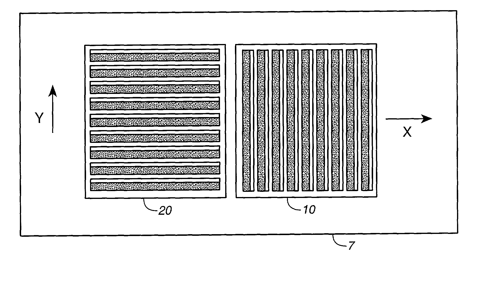
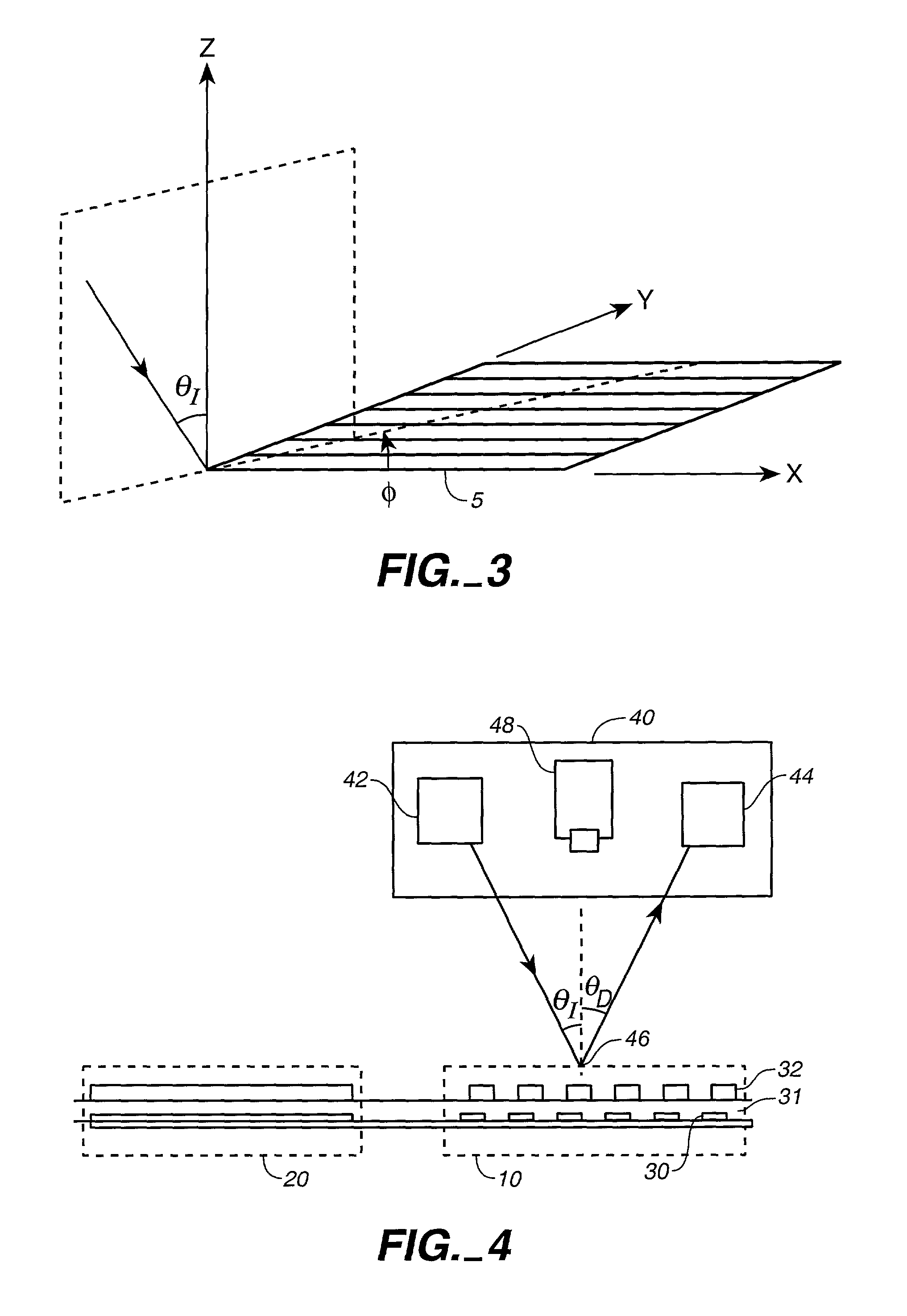
[0063] Referring to FIG. 5, in the simplest embodiment of the present invention, two test patterns 10 and 20, each having a pair of overlapping gratings, are placed in a region on the wafer that does not interfere with the devices that are being manufactured. For example, the test patterns can be placed on a scribe line 7 between the dies on a wafer. Test pattern 20 is similar to test pattern 10 rotated by 90 degrees. Each of the test patterns 10 and 20 consists of two overlying gratings 30 and 32 diagrammatically shown in cross section in FIG. 6 or 7. FIG. 7 differs from FIG. 6 only in that the line features in lower grating 30 have an asymmetric profile, e.g. due to a chemical-mechanical planarization (CMP) process. Grating 30 is formed on the lower layer, i.e., at an earlier stage of fabrication. Grating 32 is subsequently formed on the upper layer, which needs to be well aligned laterally with the lower layer. There may be one or more layers 31 between gratings 30 and 32. The up...


PUM

PropertyMeasurementUnit
wavelengthaaaaaaaaaa

Abstract

Alignment accuracy between two or more patterned layers is measured using a metrology target comprising substantially overlapping diffraction gratings formed in a test area of the layers being tested. An optical instrument illuminates all or part of the target area and measures the optical response. The instrument can measure transmission, reflectance, and/or ellipsometric parameters as a function of wavelength, polar angle of incidence, azimuthal angle of incidence, and/or polarization of the illumination and detected light. Overlay error or offset between those layers containing the test gratings is determined by a processor programmed to calculate an optical response for a set of parameters that include overlay error, using a model that accounts for diffraction by the gratings and interaction of the gratings with each others' diffracted field. The model parameters might also take account of manufactured asymmetries. The calculation may involve interpolation of pre-computed entries from a database accessible to the processor. The calculated and measured responses are iteratively compared and the model parameters changed to minimize the difference.

Description

[0001] This patent application claims priority under 35 U.S.C. .sctn.119(e) from prior U.S. provisional applications nos. 60 / 268,485, filed Feb. 12, 2001, 60 / 295,111, filed Jun. 1, 2001, and 60 / 322,219, filed Sep. 14, 2001.[0002] This invention relates to measuring the pattern overlay alignment accuracy of a pair of patterned layers on a semiconductor wafer, possibly separated by one or more layers, made by two or more lithography steps during the manufacture of semiconductor devices.[0003] Manufacturing semiconductor devices involves depositing and patterning several layers overlaying each other. For example, gate interconnects and gates of a CMOS integrated circuit have layers with different patterns, which are produced by different lithography stages. The tolerance of alignment of the patterns at each of these layers can be smaller than the width of the gate. At the time of this writing, the smallest linewidth that can be mass produced is 130 nm. The state of the art mean +3.sigm...

Claims


Application Information

Patent Timeline
Patent Type & Authority Applications(United States)
IPC IPC(8): G03F7/20H01L23/544
CPCG03F7/70633H01L2223/54453H01L22/34
Inventor SEZGINER, ABDURRAHMANJOHNSON, KENNETH C.STANKE, FRED E.
Owner TOKYO ELECTRON LTD
Why Eureka
Try Eureka