

Coating material and photovoltaic element
a photovoltaic element and coating material technology, applied in the direction of pv power plants, transportation and packaging, synthetic resin layered products, etc., can solve the problems of reducing conversion efficiency, reducing productivity, and varying characteristics of elements, and achieve high workability and production cost
Inactive Publication Date: 2002-12-12
CANON KK
View PDF0 Cites 17 Cited by
- Summary
- Abstract
- Description
- Claims
- Application Information
AI Technical Summary
Benefits of technology
[0019] In addition, other characteristics and advantageous effects of the present invention will be described later in detail.
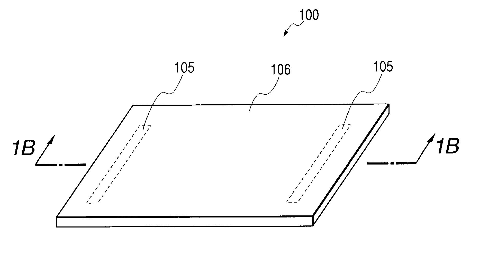
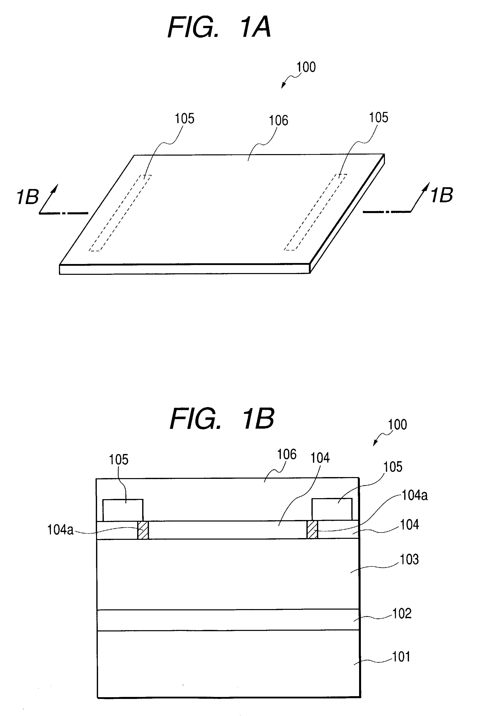
[0020] FIG. 1A is a perspective view of a photovoltaic element according to an embodiment of the present invention; and
[0021] FIG. 1B is a sectional view taken along the line 1B-1B of FIG. 1A.
[0022] Although embodiments of a preferable coating material and a preferable photovoltaic element according to the present invention will be described below in detail, the present invention is not limited to these embodiments at all.
[0023] FIGS. 1A and 1B show an example of the photovoltaic element of the present invention. FIG. 1A is a perspective view of the photovoltaic element, and FIG. 1B is a sectional view taken along the line 1B-1B of FIG. 1A. FIGS. 1A and 1B show a photovoltaic element 100, an electroconductive base member 101, a back side reflective layer 102, a semiconductor photo-active layer 103, a transparent electroconductive layer 104, a collecting electrode 105, and an optical diffusion layer 106 consisting of a coating material according to the present invention. Reference character 104a denotes each a section where the transparent electroconductive layer is removed.Photovoltaic Element 100
[0024] A general photovoltaic element can be suitably used for the photovoltaic element 100 of the present invention. It is possible to produce the photovoltaic element of the present invention by coating at least a part of a light-receiving plane side of the photovoltaic element 100 with a resin described later.
Problems solved by technology
However, the texture structure having physical unevenness has a problem of causing the reduction of productivity and the variation of characteristics between the elements due to the defects of the photoelectric conversion layer particularly in a convex portion or the variation of the film thickness of the photoelectric conversion layer.
In addition, the junction breaking between a photoelectric conversion layer and an electrode, leakage of a current, ohmic loss, etc. generate and hence may cause the decrease of a conversion efficiency.
Furthermore, such techniques have a problem that plant-and-equipment investment requires immense costs.
However, since an optical diffusion layer is formed with the resin which is mixed with the particles or filler, long-term use under harsh environments such as the outdoors causes peeling in a boundary between the resin and an insoluble resin or additives such as particles, and plenty of minute air layers generate in the optical diffusion layer.
For example, since the light which enters on a non-power-generating region in a light-receiving plane side of the photovoltaic element usually goes straight on, it cannot contribute to power generation.
If more than 1000, phase separation with the first polymeric material arises, which causes deterioration of durability.
Since the number-average molecular weight of less than 250 becomes insufficient in light scattering, there is a possibility that a desired optical confinement effect may not be exerted.
If fewer than 0.1 parts by weight, there is a possibility that no desired optical confinement effect may be exerted.
If larger than 90 mg / KOHmg, crosslinking becomes excessive, a coating film becomes hard, and hence, this becomes weak at an outdoor temperature change.
Method used
View moreImage
Smart ImageViewing Examples

Examples
example 2
[0077] Photovoltaic elements was produced and evaluated similarly to Example 1 except that a crosslinking material made of methylated melamine, and curing temperature of 120.degree. C. were used. The evaluation results are shown in Table 1.
example 3
[0078] The photovoltaic elements were produced and evaluated similarly to Example 1 except that instead of the second polymeric material (1) in the Example 1, the second polymeric material (2) (hydroxyl value 30 mg / KOH) made by bonding a polymer component, which was polymerized from several kinds of monomers having vinyl group, and a polymer component including fluorine (fluorine content: 45%, average molecular weight: 5,000) was used. The evaluation results are shown in Table 1.
Login to View More PUM
| Property | Measurement | Unit |
|---|---|---|
| mole ratio | aaaaa | aaaaa |
| mole ratio | aaaaa | aaaaa |
| light transmittance | aaaaa | aaaaa |
Abstract
The present invention provides a coating material which resin-coats a light-receiving plane side of a photovoltaic element, and which can increase a conversion efficiency by effectively using light incident on the photovoltaic element and is excellent in weatherability since the coating material comprises a resin which is a polymer blend containing at least a first polymeric material, and a second polymeric material made by bonding a polymer component (A) and a polymer component (B), wherein the polymer component (A) includes a functional group with comparatively high compatibility with the first polymeric material, and a polymer component (B) includes a functional group with compatibility with the first polymeric material which is lower than the compatibility of the functional group of the polymer component (A), and wherein the polymer component (B) forms an aggregate.
Description
[0001] 1. Field of the Invention[0002] The present invention relates to a coating material and a photovoltaic element, and in particular, to a photovoltaic element whose light-incident side is resin-coated.[0003] 2. Related Background Art[0004] There is a technique which forms a photovoltaic element on a substrate having physical unevenness, which is called texture, as one of means for increasing a conversion efficiency (electric output) of the photovoltaic element.[0005] For example, there are a method of unevenly forming an ITO film or an SnO.sub.2 film on flat glass, and making its surface uneven (Japanese Patent Publication No. 57-31312), formation of a rough surface by sand blasting or sputtering of a substrate (Japanese Patent Publication No.58-176101), and a photovoltaic element substrate on which a surface of a metal thin film formed by plasma CVD etc. has texture structure (Japanese Patent Publication No. 01-31946). All of these are techniques of increasing the total quanti...
Claims
Login to View More Application Information
Patent Timeline
 Patent Type & AuthorityApplications(United States)
IPC IPC(8): C08L83/04C09D157/00C09D133/04C09D183/04C09D183/07C09D201/02C09D201/06H01L31/04H01L31/048H01L31/052H01L31/18
CPCC08L83/04C09D133/04H01L31/048H01L31/056H01L31/1884Y02E10/52C08L83/00H01L31/02168Y10T428/31663Y10T428/31855Y10T428/31573
InventorSHIOTSUKA, HIDENORITAKABAYASHI, AKIHARUKATAOKA, ICHIRO
OwnerCANON KK