

Method for manufacturing microstructure, method for manufacturing liquid discharge head, and liquid discharge head
- Summary
- Abstract
- Description
- Claims
- Application Information
AI Technical Summary
Benefits of technology
Problems solved by technology
Method used
Image

Examples
first embodiment
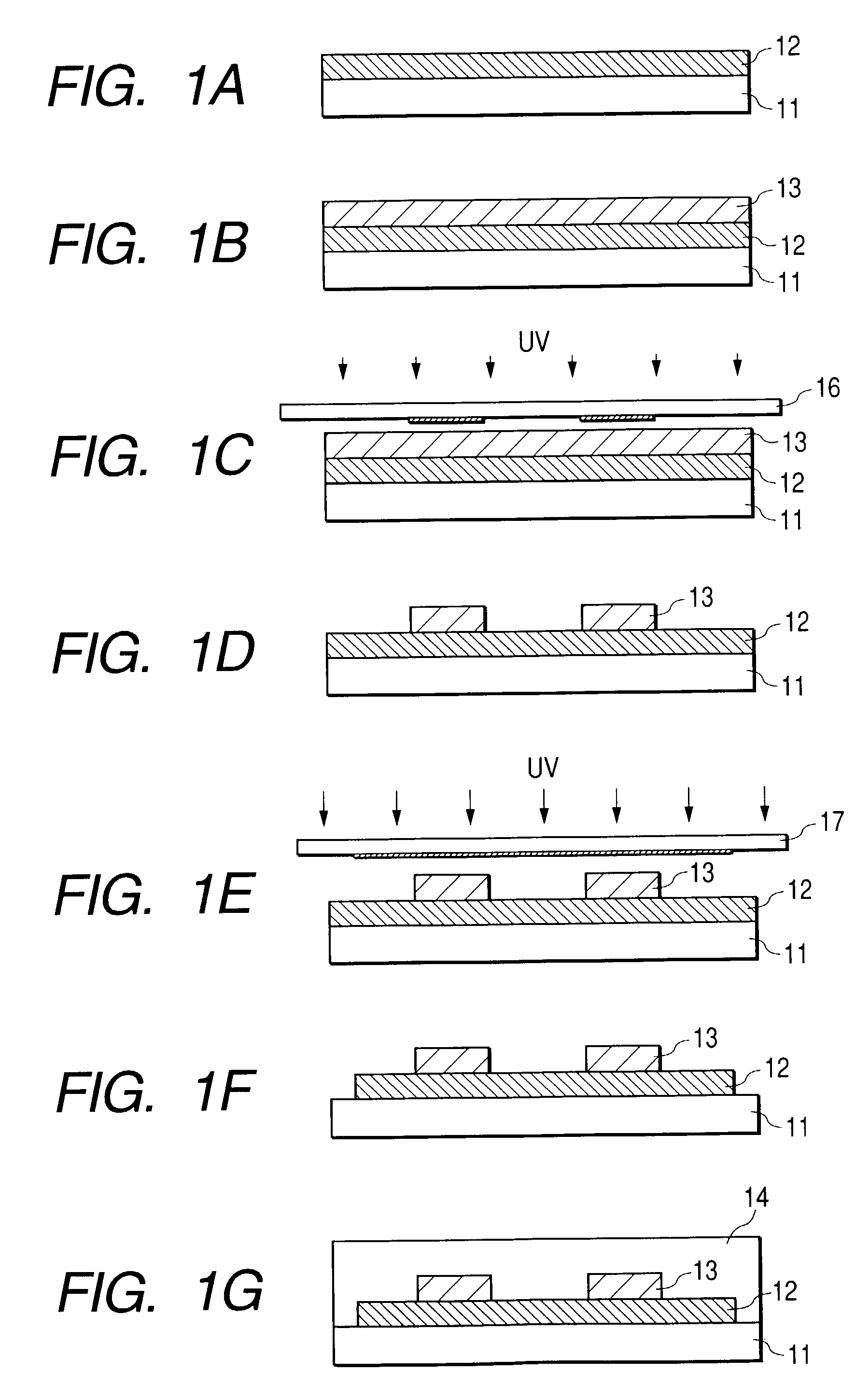
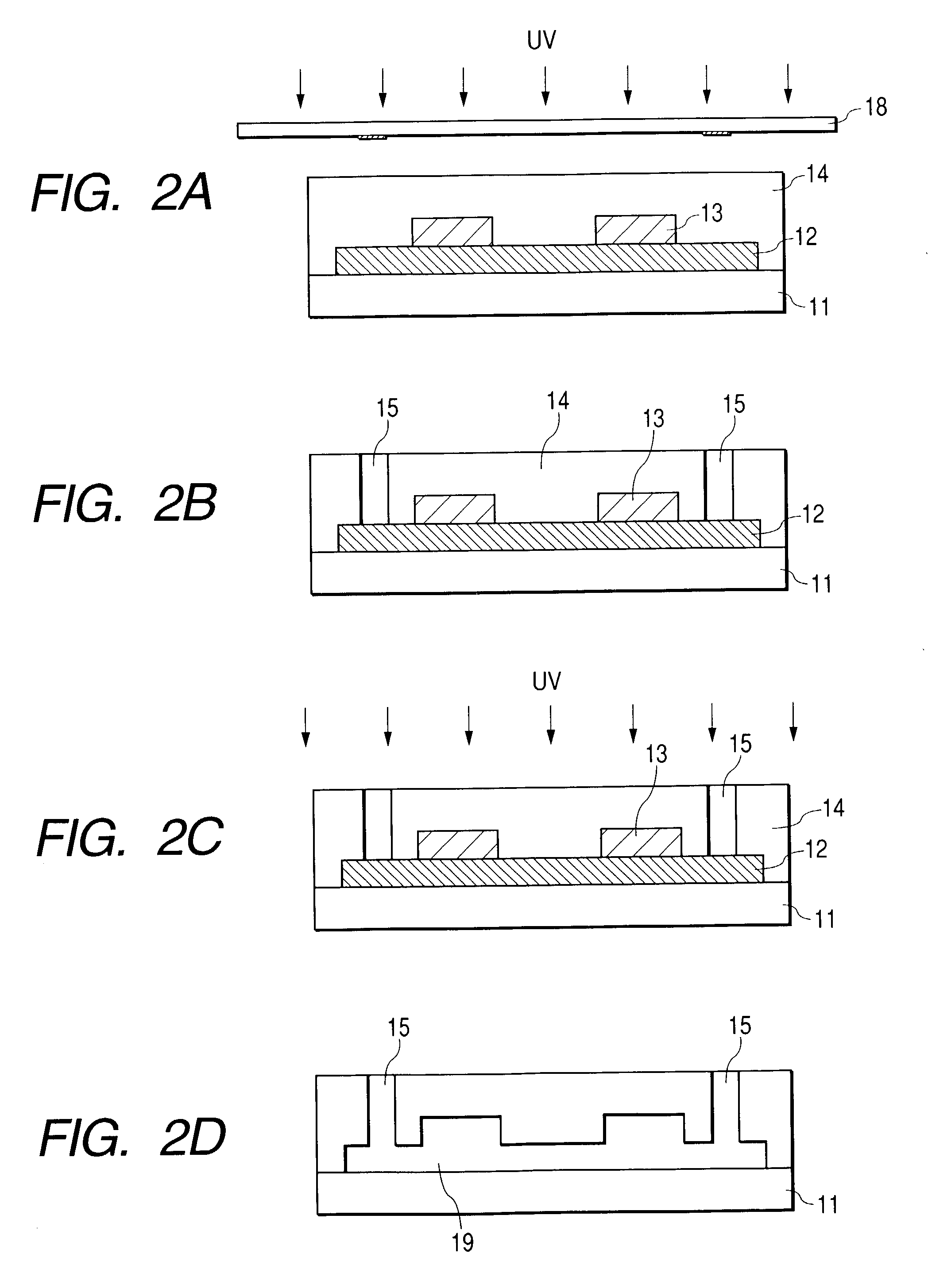
[0123] (First Embodiment)
[0124] FIG. 10 to FIG. 19 are views each showing one example of the structure of liquid discharge recording head and the manufacturing procedures therefore, which are related to the method embodying the present invention. Here, in each of the examples, a liquid discharge recording head, which is provided with two orifices (discharge ports), is represented, but it is needless to mention that the invention is equally applicable to a high-density, multiply arrayed liquid discharge recording head, which is provided with orifices in a number more than two.
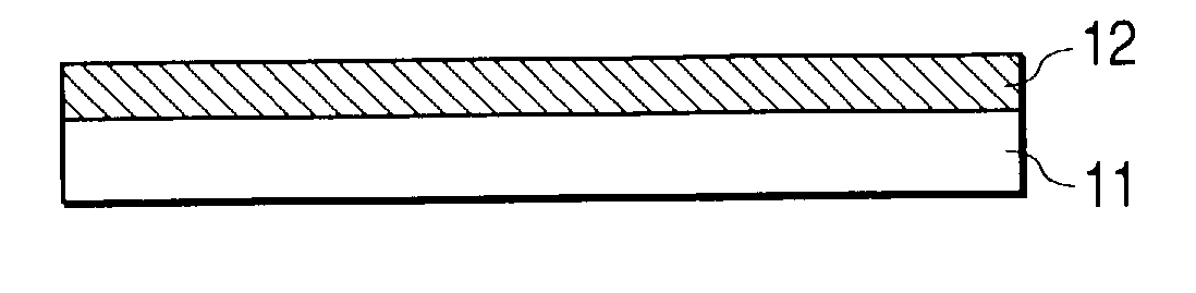
[0125] At first, for the present embodiment, a base plate 201 formed by glass, ceramics, plastic, metal, or the like is used as shown in FIG. 10, for example.
[0126] Here, FIG. 10 is a view that schematically shows the base plate before the layer of photosensitive material is formed.
[0127] The base plate 201 of the kind can be used without any particular limitation as to the configuration, material, and the like ...
second embodiment
[0143] (Second Embodiment)
[0144] The present embodiment describes a modal example in which methacrylate, which is not thermo-bridge type, is used for the lower layer resist. Here, however, the best mode is the one that uses the thermo-bridge type described in the first embodiment.
[0145] Now, the description is given below. At first, as the lower layer, polymethyl methacrylate (PMMA) is formed on the base plate in the same manner as the first embodiment.
[0146] PMMA is prepared for use by adjusting the ODUR-1000, which is product number on the market by Tokyo Oka Kogyo K.K., to the solid portion by concentration of 20 wt %. Next, PMIPK film is formed on the PMMA film by use of laminating method.
[0147] Here, on the polyethylene terephthalate film (thickness: 25 .mu.m), which is given mold-strip treatment, PMIPK is coated by use of a roller coater to prepare the dry film thereof. The basic film is on the market by Teijin K.K., and the one that has the mold-strip treatment grade of A-53 ...
third embodiment
[0151] (Third Embodiment)
[0152] By the method of manufacture of the first embodiment, an ink jet head is produced in a structure as shown in FIG. 6A. As shown in FIGS. 20A and 20B, in accordance with the present embodiment, the horizontal distance from the opening edge 42a of the ink supply port 42 to the edge 47a of the discharge chamber 47 on the ink supply port side is 100 .mu.m for this ink jet head. The ink flow path wall 46 is formed from the edge 47a of the discharge chamber 47 on the ink supply port side to a location at 60 .mu.m on the ink supply port 42 side, and divides the respective discharge elements. Also, the height of the ink flow path is arranged to be 10 .mu.m over the portion of 10 .mu.m from the edge 47a of the discharge chamber 47 on the ink supply port side to the ink supply port 42 side, and 20 .mu.m on the other portions. The distance from the surface of the base plate 41 to the surface of the liquid flow-path structural material 45 is 26 .mu.m.
[0153] FIG. 2...
PUM
| Property | Measurement | Unit |
|---|---|---|
| Microstructure | aaaaa | aaaaa |
| Wavelength | aaaaa | aaaaa |
| Energy | aaaaa | aaaaa |
Abstract
Description
Claims
Application Information