Plasma display panel and method for its manufacure

a technology of plasma display panel and manufacure, which is applied in the manufacture of electric discharge tubes/lamps, cold cathode manufacturing, and electromechanical systems, etc., can solve the problems of increasing the depth and weight of crt televisions, difficult to produce large-screen lcds, and inconvenient production of crts. achieve good luminance efficiency and low manufacturing cost

Inactive Publication Date: 2003-02-27
PANASONIC CORP
View PDF1 Cites 25 Cited by
  • Summary
  • Abstract
  • Description
  • Claims
  • Application Information

AI Technical Summary

Benefits of technology

[0017] It is an object of the present invention to provide a PDP that has good luminance efficiency, requires low manufacturing costs, and is protected to some extent from the yellowing of glasses and degradation of phosphors.

Problems solved by technology

However, the depth and weight of CRT televisions increase with screen size, so that CRTs are not suited to the production of large televisions with screen sizes of 40 inches or more.
As for LCDs, they have some notable advantages, such as low power consumption and low driving voltages, but it is technically difficult to produce large-screen LCDs.
This would increase power consumption of the PDP.
The power consumption of the PDP becomes particularly large when the frequency at which the PDP is driven is set at a high level, for instance at 200 KHz or more, with the aim of increasing its luminance.
Another factor that could increase PDP's power consumption is the use of a low melting-point glass for the ribs.
These compounds tend to react with transparent electrodes (ITO), and damage their conductivity.
Then, it becomes difficult to drastically reduce dielectric constant of the whole dielectric layer.
Another challenge in forming dielectric layers and ribs from a low melting-point glass is cost.
After the low melting-point glass is applied, the glass is sintered at temperatures 500-600 degrees C. But this sintering process requires substantial amount of time and energy, and it has been requested to reduce that time and energy and manufacturing costs.
However, it is difficult in terms of time and cost to produce 20-30 .mu.m thick films with deposition and sputtering method.
In addition, there is a higher likelihood of cracks being formed in SiO.sub.2 layers that have grown more than 10 .mu.m thick.
Therefore, it seems virtually impossible to reduce capacitance of dielectric layers if they are made of SiO.sub.2.

Method used


Image

  • Plasma display panel and method for its manufacure
  • Plasma display panel and method for its manufacure
  • Plasma display panel and method for its manufacure

Examples


Embodiment Construction

[0132]

2TABLE 1

[0133] Actual Example PDPs No.1-5 are produced in accordance with the description about the above embodiment, which are shown in Table 1.

[0134] The first dielectric layers of these actual examples are made of silicones whose thicknesses are shown in Table 1. The second dielectric layers and ribs are made from a mixture of polymethylsiloxane resin and SiO.sub.2.

[0135] The materials for the dielectric layer and ribs are applied by process printing or spin coat method.

[0136] The example PDP No. 6 is a comparison example whose dielectric layers and ribs are made of PbO glass (with a dielectric constant of 11).

[0137] The following describes the specification used commonly for the actual and comparison examples.

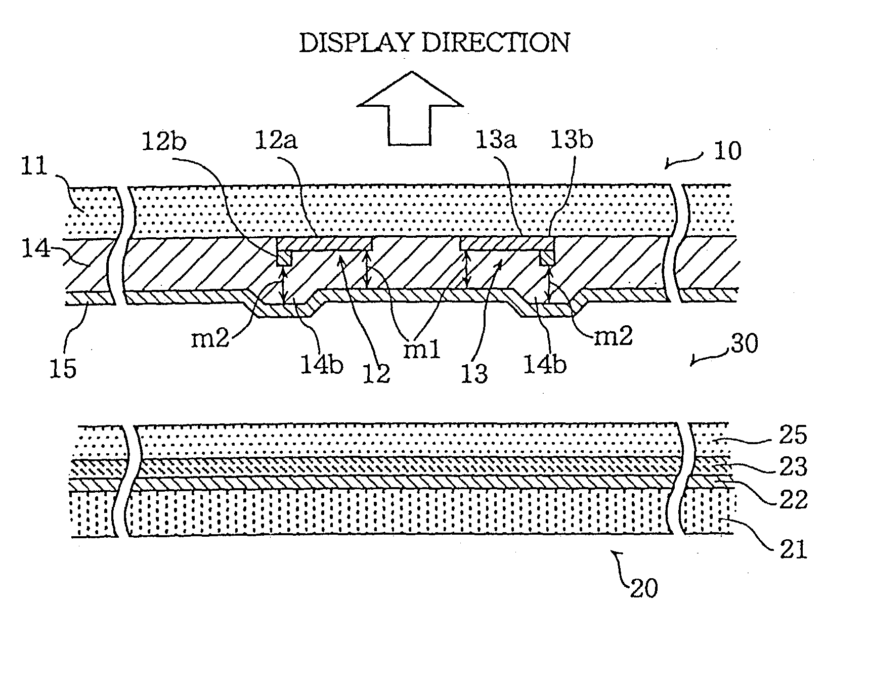
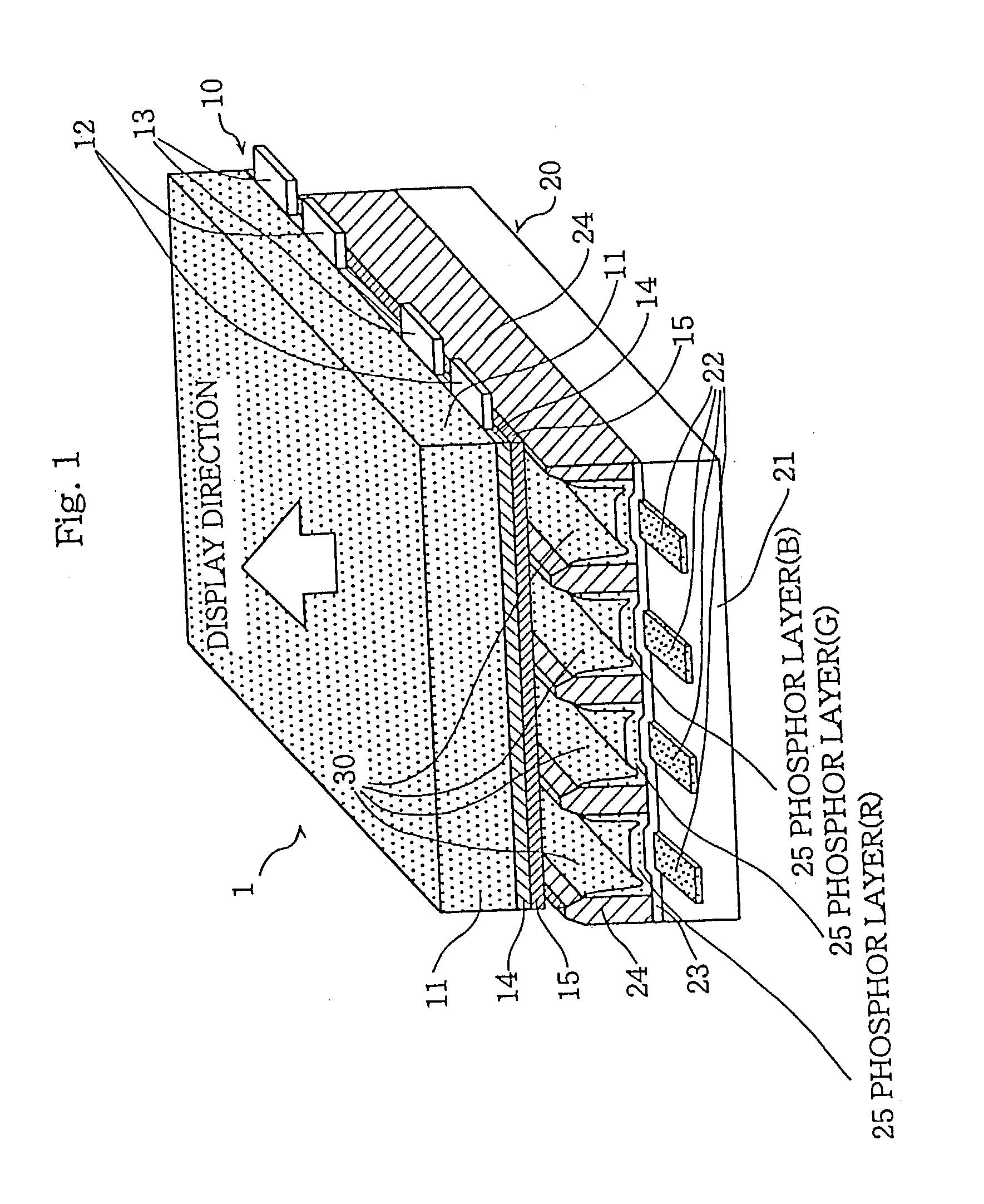
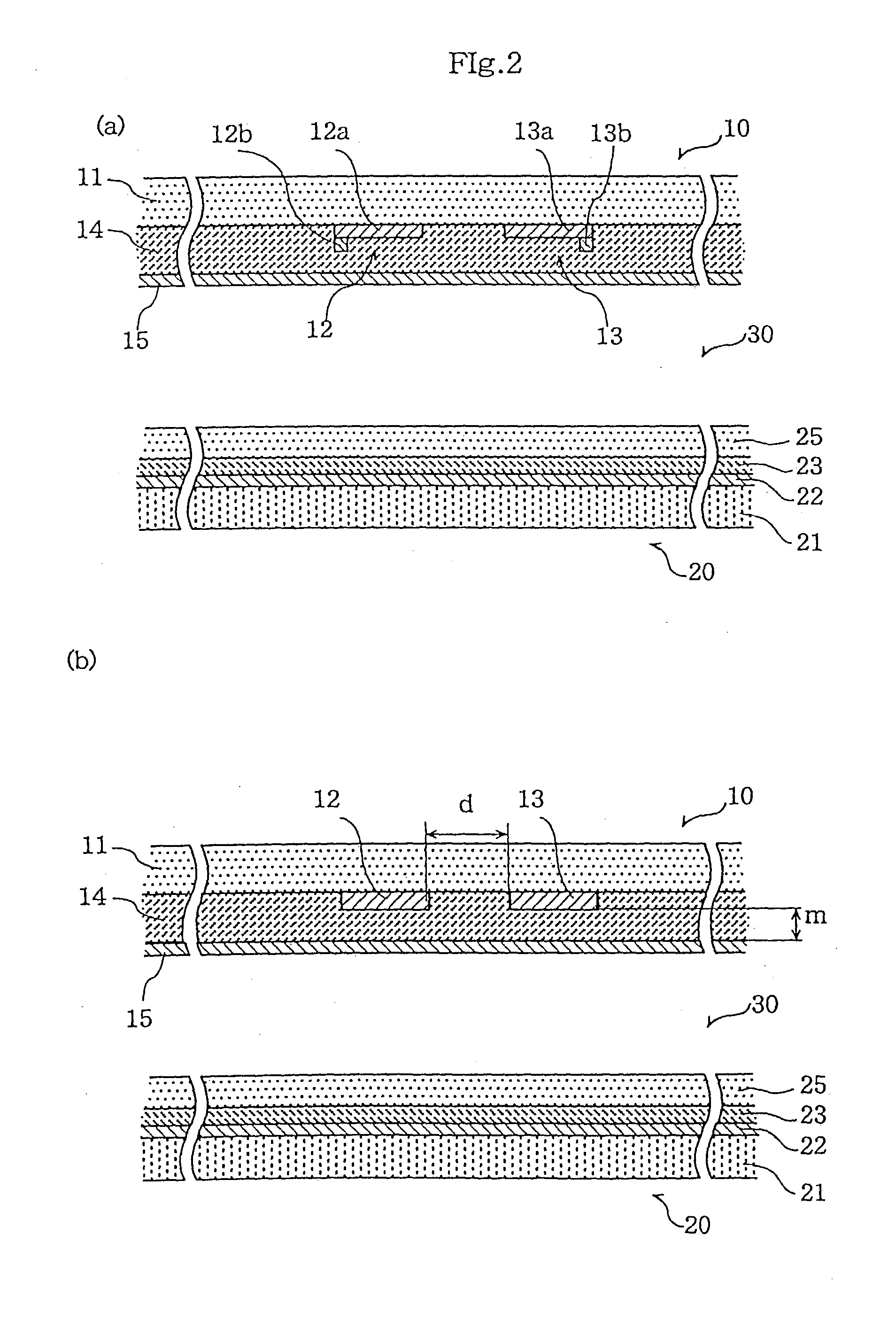
[0138] The front glass plate and the back glass plate are a 2 mm thick soda lime glass plate. The cell size of these PDPs is determined according to a 42-inch VGA display; the ribs 24 are 0.15 mm high, the distance between any neighboring ribs 24 (cell pitch) is 0.36 ...


PUM

PropertyMeasurementUnit
dielectric constantaaaaaaaaaa
sizesaaaaaaaaaa
dielectric constantaaaaaaaaaa

Abstract

A plasma display panel that requires lower consumption power to drive is proved. This plasma display has a good luminance efficacy, is less tending to yellowing of glass and deterioration of phosphors, and is manufactured at a low cost. The dielectric layers and ribs of the PDP are made from a silicone resin containing polysiloxane bond. Preferably, the silicon resin should have siloxane bond joined with methyl group, ethyl group or phenyl group. It is also preferable that a sealing member is made from a silicone resin.

Description

[0001] The present invention relates to a plasma display panel for use in color television sets.[0002] In recent years, there has been a growing demand for the realization of large-screen televisions with superior quality. One example of such televisions is televisions for the "HiVision" standard used in Japan. In the field of display devices, development has been underway for a variety of display devices, such as CRTs, liquid crystal displays (hereafter referred to as LCD) and plasma display panels (hereafter referred to as PDP) with the aim of producing suitable televisions.[0003] CRTs have been conventionally used as displays of televisions and offered superior resolution and picture quality. However, the depth and weight of CRT televisions increase with screen size, so that CRTs are not suited to the production of large televisions with screen sizes of 40 inches or more. As for LCDs, they have some notable advantages, such as low power consumption and low driving voltages, but i...

Claims


Application Information

Patent Timeline
Patent Type & Authority Applications(United States)
IPC IPC(8): H01J9/02H01J9/24H01J9/26H01J17/16H01J17/49
CPCH01J9/02H01J9/241H01J9/242H01J9/261H01J11/12H01J11/36H01J11/38H01J2211/366H01J9/24
Inventor AOKI, MASAKIWATANABE, TAKU
Owner PANASONIC CORP
Why Eureka
Try Eureka