Variable resistor structure and method for forming and programming a variable resistor for electronic circuits

a variable resistor and electronic circuit technology, applied in the direction of semiconductor devices, semiconductor/solid-state device details, electrical apparatus, etc., can solve the problems of inability to manufacture features and devices near the fuses, damage to surrounding circuitry, and penalties incurred

Inactive Publication Date: 2003-11-20
IBM CORP
View PDF0 Cites 43 Cited by
  • Summary
  • Abstract
  • Description
  • Claims
  • Application Information

AI Technical Summary

Problems solved by technology

However, there is an area penalty incurred on the chip by the inclusion of the redundant circuitry, and damage may result to the surrounding circuitry.
A drawback with this method is that the area required by the region damaged by ablation is relatively large, so that features and devices cannot be fabricated near the fuses.
Another drawback with laser-ablated fuses is that they do not scale well with lithography.
The damage to such back-end structures poses reliability concerns, such as the electrical shorting of elements that the manufacturer does not intend to be shorted.
Damage resulting from blowing fuses also imposes limits on the proximity of adjacent fuses, and hence fuse pitch reduction which directly affects circuit packing density, and which may be cumulative to the area penalty imposed by the inclusion of the redundant circuitry.
The damage and debris that occurs around the programmed link after ablation can limit the achievable pitch in manufacturing the device and, consequently, the level of integration and miniaturization.
Therefore, both the ultimate scalability and reliability of the device are necessarily affected adversely by conventional approaches to programming a fuse.
The technology used for integrated circuit manufacturing is migrating to low k and ultra low k materials which are mechanically very weak and very susceptible to damage from disruptive fuse programming like ablation.
The use of fusible links for device personalization has further inherent limitations.
Specifically, the fuse link can only be blown open or left closed; they

Method used


Image

  • Variable resistor structure and method for forming and programming a variable resistor for electronic circuits
  • Variable resistor structure and method for forming and programming a variable resistor for electronic circuits
  • Variable resistor structure and method for forming and programming a variable resistor for electronic circuits

Examples


Embodiment Construction

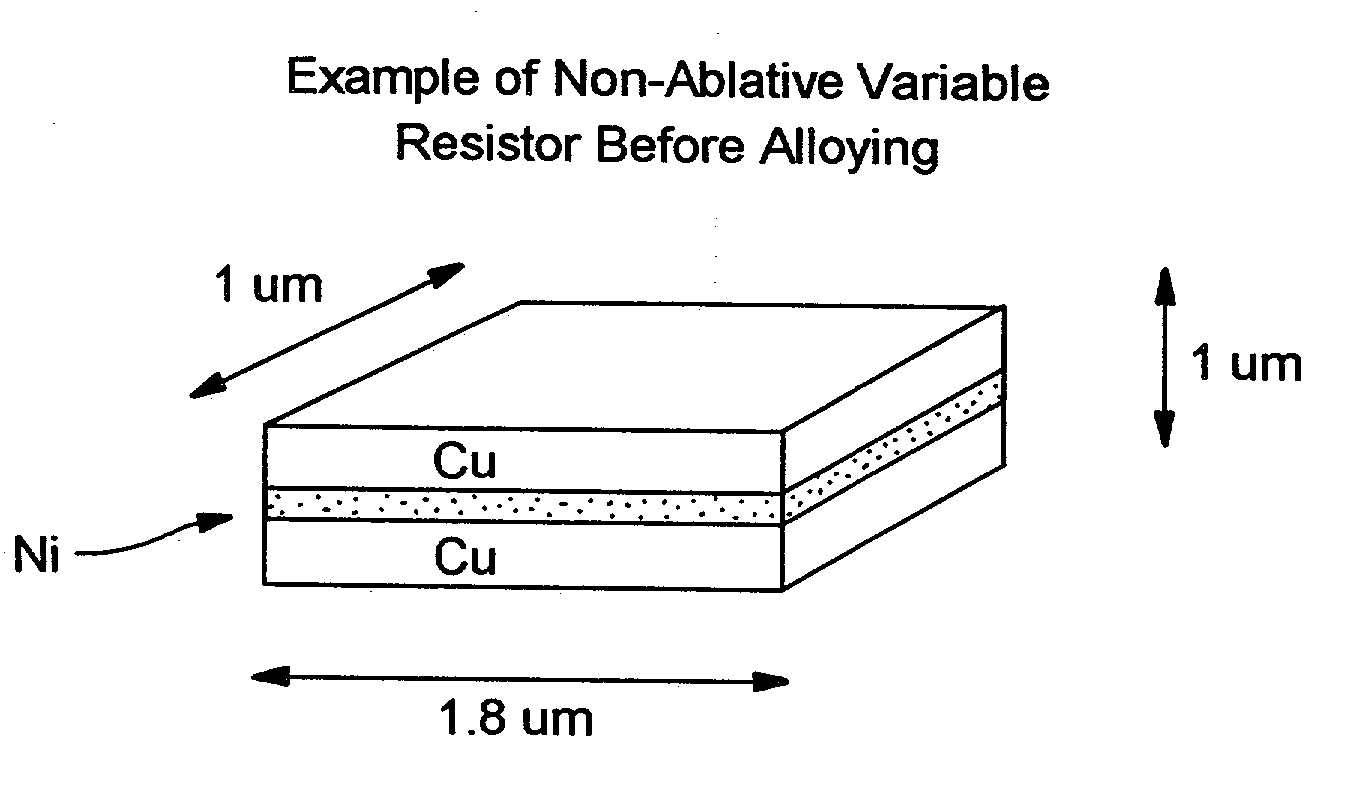
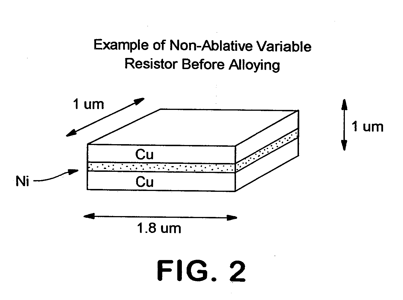
[0053] We have found that a variable resistor having an adjustable, precisely determined value that can be can be reliably and repeatedly manufactured can be obtained by using a lamination of two or more conductive materials, e.g., metals, that are subsequently at least partially alloyed. This non-ablative structure and method overcomes the problems associated with conventional approaches in programmable elements and impedance trimming, as discussed above.

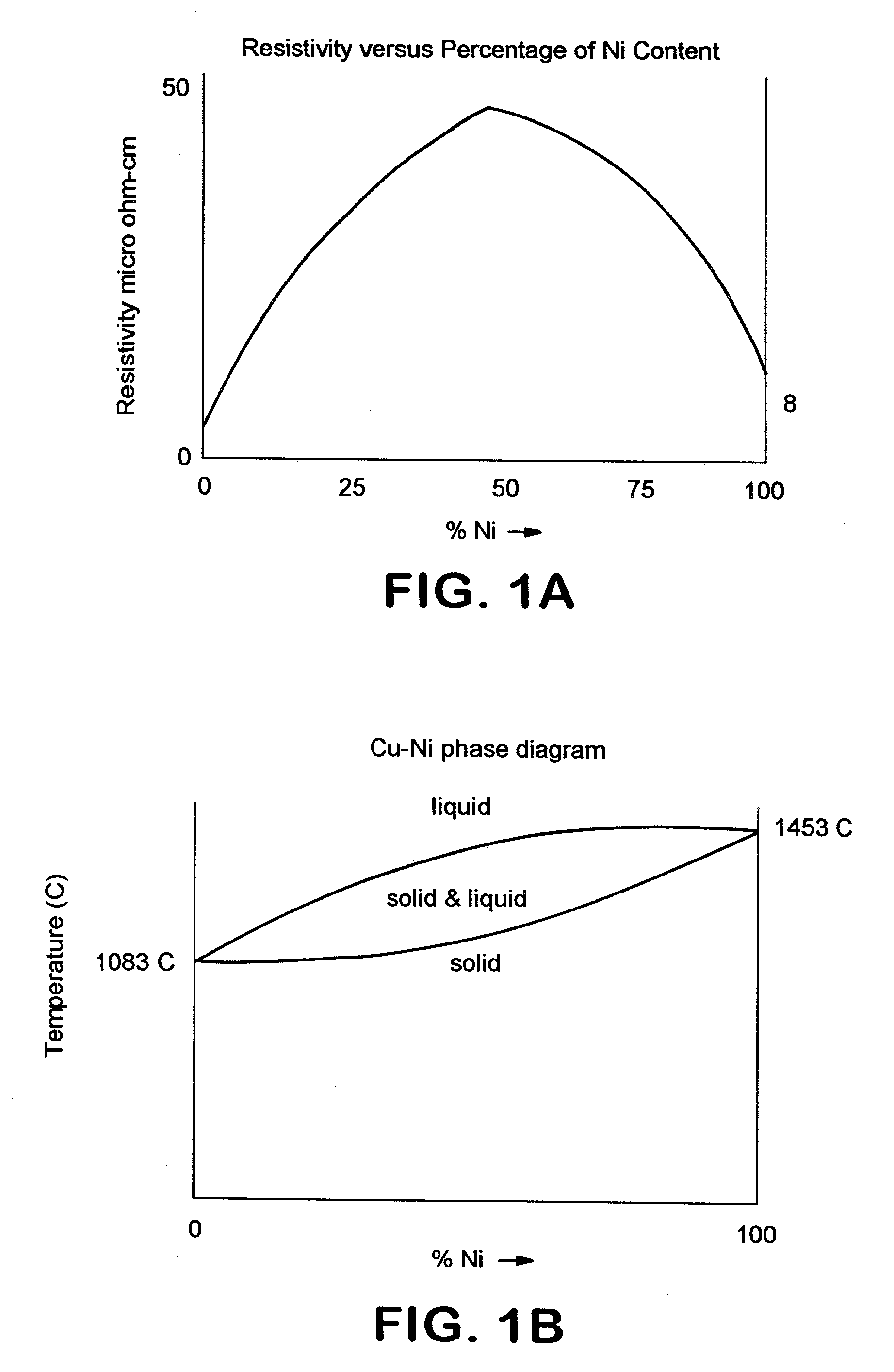
[0054] Alloying two metals increases the resistance of the resulting alloy to a value greater than the resistance of either of the base metals. For example, in one embodiment, a lamination of copper (Cu) and nickel (Ni) are interdiffused to increase a resistor having a higher resistance than the original lamination before alloying.

[0055] One metal system ideally suited to this invention is the Cu--Ni system. Copper is a preferred metal of choice in BEOL interconnects wiring associated with high performance integrated circuits, espe...


PUM


Abstract

A non-ablative structure and method for forming a variable resistor includes providing a programmable resistive element including two or more different conductive materials, and changing a resistance of the programmable resistive element to a finite value by heating the programmable element by either providing a current flow through the programmable element, or directing a laser beam onto the programmable element. The conductive materials are interdiffused to form an alloy of the conductive materials. A resistance value of the variable resistor is determined, at least in part, by the degree to which the conductive materials are alloyed or interdiffused. The method and structure of the variable resistor prevents ablative damage to adjoining circuit structure, allowing tighter pitch, and has application to digital programmable elements, and to resistance trimming for impedance matching in RF integrated circuits.

Description

[0001] 1. Field of the Invention[0002] The present invention relates to a structure and method for forming a controllably variable resistor having wide application to a variety of unique digital and analog circuits, including both programmable digital integrated circuit devices, and programmable analog integrated circuit devices.[0003] The present invention even more particularly relates to a structure and method for forming and setting a programmable resistive element such as a fuse or antifuse used in programming digital integrated circuit devices including redundant memory elements, for example. This invention also relates to a programmable or trimming resistor used in analog RF circuit tuning applications. More specifically, this disclosure relates to a structure and method for non-ablatively forming a fuse, antifuse, or trimming resistor element without ablation by selectively altering resistivity of the variable resistor to a finite value.[0004] 2. Description of Related Art[0...

Claims


Application Information

Patent Timeline
IPC IPC(8): H01L23/525
CPCH01L23/5252H01L23/5254H01L2924/3011H01L23/5258H01L23/5256H01L2924/0002H01L2924/00
Inventor HSU, LOUIS LU-CHENNARAYAN, CHANDRASEKHARRADENS, CARL J.
Owner IBM CORP
Why Eureka
Try Eureka