

Method and apparatus for position measurement of a pattern formed by a lithographic exposure tool
a technology of lithographic exposure and position measurement, which is applied in the direction of semiconductor/solid-state device testing/measurement, semiconductor/solid-state device details, instruments, etc., can solve the problems of reduced signal propagation time, increased circuit complexity and additional signal processing functions to be provided, and inability to ensure the flatness of the image field at the targ
- Summary
- Abstract
- Description
- Claims
- Application Information
AI Technical Summary
Benefits of technology
Problems solved by technology
Method used
Image

Examples
Embodiment Construction
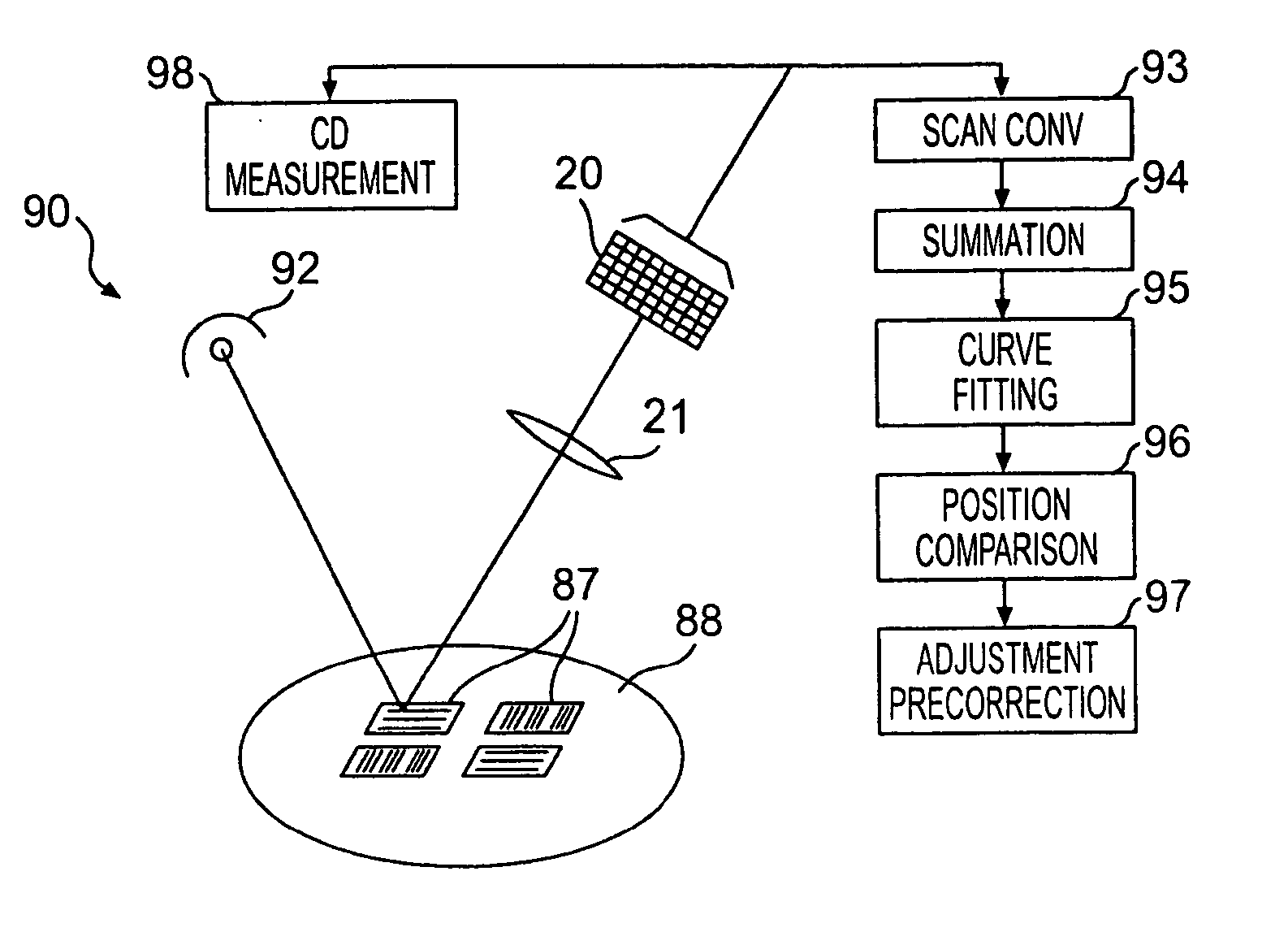
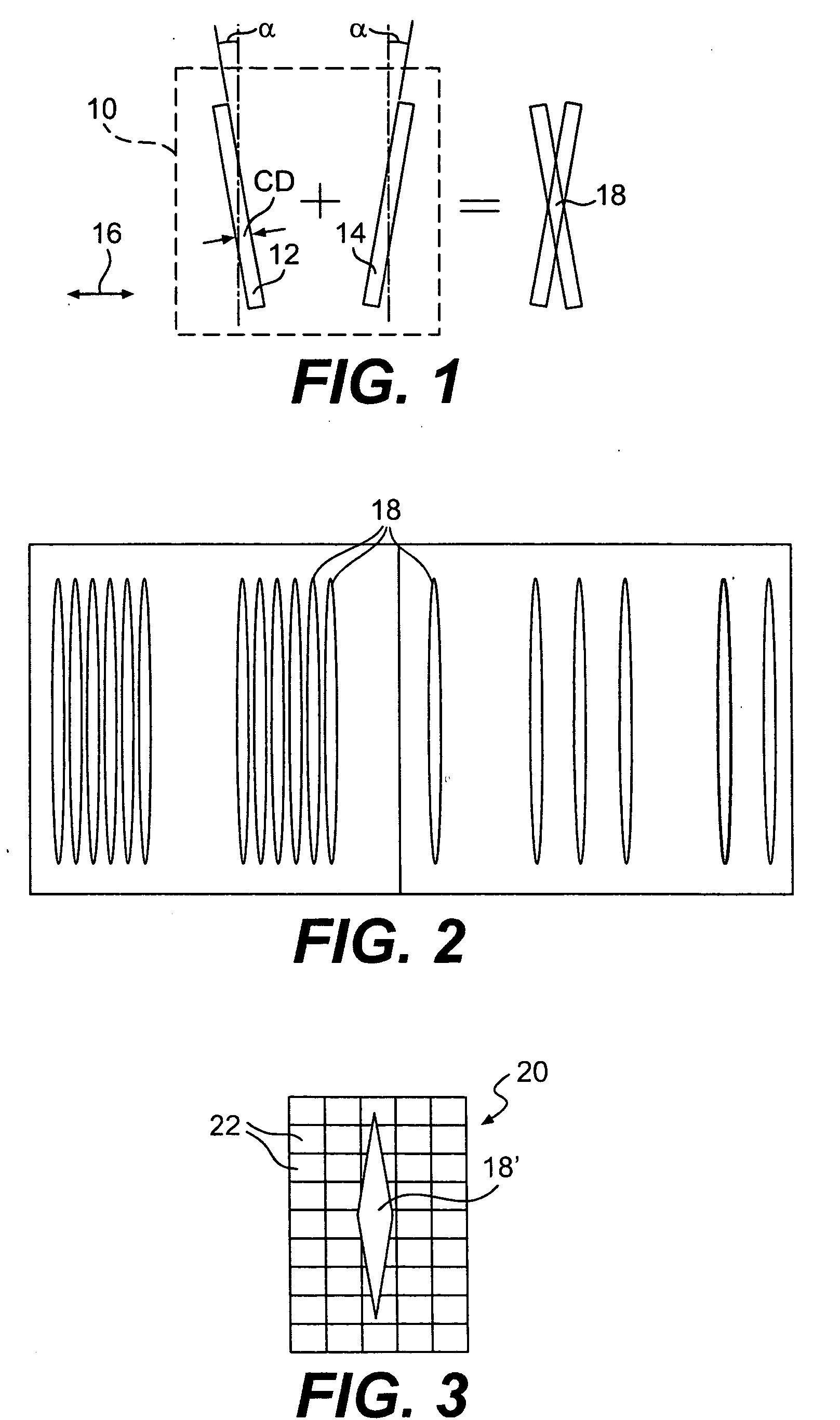
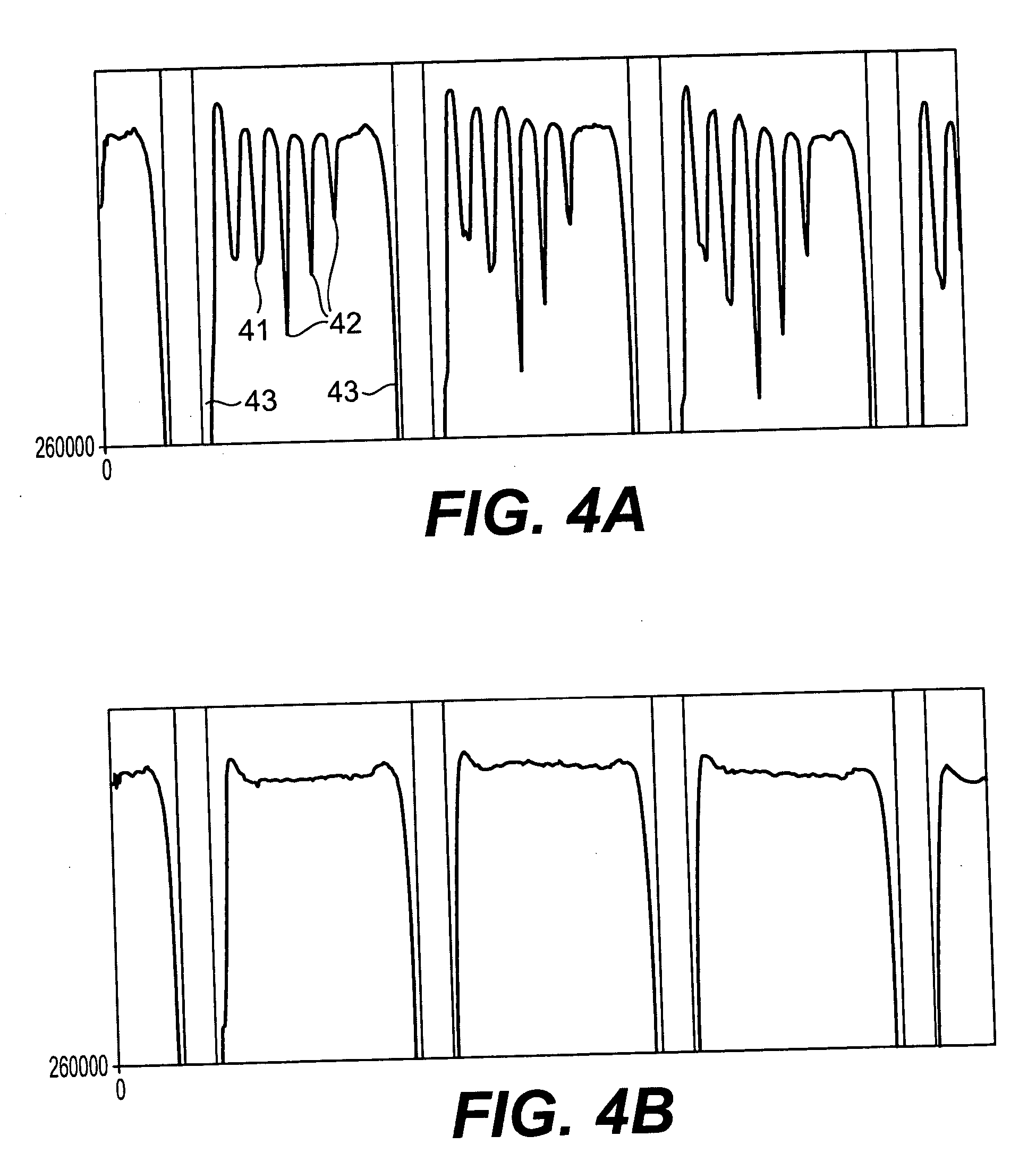
[0027] Referring now to the drawings, and more particularly to FIG. 1, there is shown a preferred imaging technique for forming a preferred type of mark for the practice of the invention. This type of mark and this technique of its formation is disclosed in U.S. Pat. No. 6,094,256 and U.S. patent application Ser. No. 09 / 861,541, both assigned to the assignee of the present application and both being hereby fully incorporated by reference herein. This type of mark and the technique of its formation are preferred largely because of the simplicity and repeatability thereof as well as the ease and consistency of extraction of information therefrom. However, it should be appreciated that the technique of such data extraction differs substantially in the patent, the patent application and the present invention, depending on the parameter of interest.
[0028] Specifically, U.S. Pat. No. 6,094,256, however, teaches use of a measurement of a length much larger than the critical dimension (embo...
PUM
| Property | Measurement | Unit |
|---|---|---|
| depth | aaaaa | aaaaa |
| depth | aaaaa | aaaaa |
| depth | aaaaa | aaaaa |
Abstract
Description
Claims
Application Information