Wafer bonding of thinned electronic materials and circuits to high performance substrates

a technology of thin-film electronic materials and substrates, applied in the direction of material nanotechnology, semiconductor devices, semiconductor/solid-state device details, etc., can solve the problems of poor quality factor, poor performance of microwave circuit applications, and loss of microwaves in transmission lines

Inactive Publication Date: 2004-01-15
THE UNITED STATES OF AMERICA AS REPRESENTED BY THE SECRETARY OF THE NAVY
View PDF15 Cites 298 Cited by
  • Summary
  • Abstract
  • Description
  • Claims
  • Application Information

AI Technical Summary

Problems solved by technology

However, their performance in microwave circuit applications suffers because of microwave losses in transmission lines and the poor quality factor ("Q") of inductors that are formed over the silicon substrate, since the silicon substrate is not obtainable as either insulating or semi-insulating.
There are microwave losses in transmission lines and degraded quality factor even in the case that a high resistivity substrate in the range of 3000-10,000 ohm-cm resistivity is used.
Semi-insulating SiC may be expensive and only available in small sizes.
Transmission line propagation issues and poor "Q" also exist for CMOS, BiCMOS, and SiGe Heterojunction Bipolar Transistor (HBT) circuits fabricated using silicon or Silicon-on-Insulator (SOI) substrates.
High speed microprocessors suffer from enhanced propagation delay in the transmission of electrical signals on metal interconnects due to microwave loss issues in the non-insulating silicon substrate.
Silicon mixed signal circuits suffer from a problem of cross talk from the digital circuit to the analog circuit.
Silicon microprocessor circuits are currently becoming thermally limited.

Method used


Image

  • Wafer bonding of thinned electronic materials and circuits to high performance substrates
  • Wafer bonding of thinned electronic materials and circuits to high performance substrates
  • Wafer bonding of thinned electronic materials and circuits to high performance substrates

Examples


Embodiment Construction

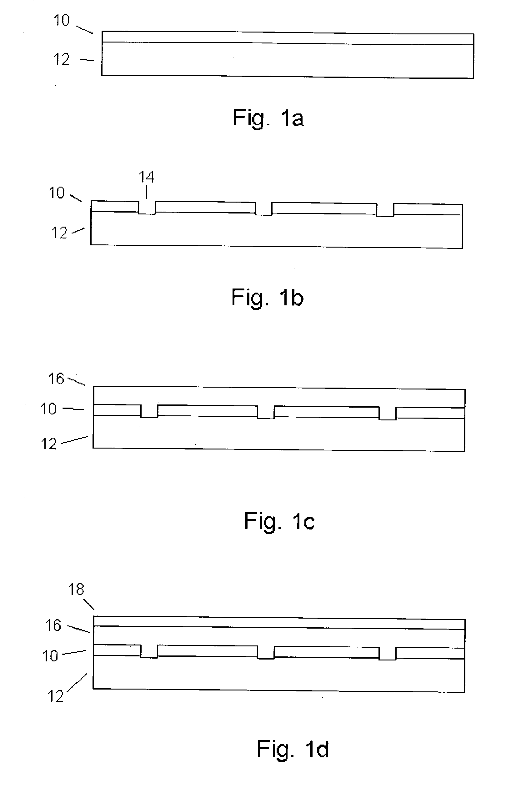
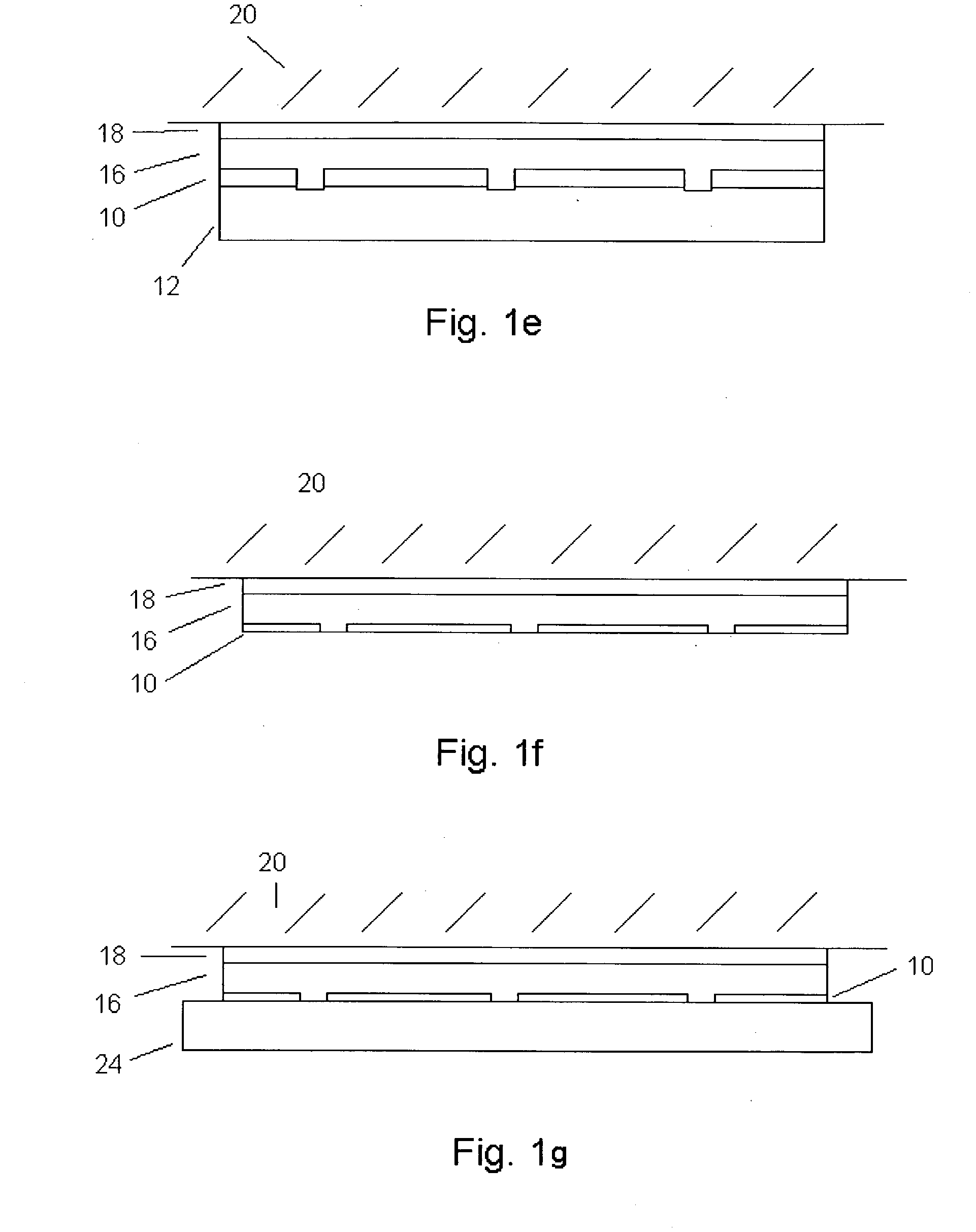
[0013] The invention comprises a method of bonding a semiconductor wafer to substrate, specifically a high performance substrate for microelectronic and / or microwave material layers, devices, or circuits. The high performance substrate may provide microelectronic or microwave material layers, devices, or circuits with a microwave insulating, a high thermal conductivity substrate, or both microwave insulating and highly thermally conductive. The high performance substrate may also be optically transparent.

[0014] The approach comprises substantially removing a large portion of the wafer upon which microelectronic or microwave materials, devices, or circuits are fabricated by thinning (optionally with the use of an etch stop layer) and then wafer bonding a high performance substrate (single crystal, polycrystalline, or composite polycrystalline substrate) to the backside of the wafer. The high performance substrate can be either microwave insulating, highly thermally conductive, optica...


PUM


Abstract

A method of bonding a wafer to a substrate comprising the steps of: providing a wafer having a front surface and a back surface; attaching the front surface of the wafer to a support; thinning the wafer from the back surface; bonding the back surface of the wafer to a substrate using a thin bonding technique; and removing the support from the front surface of the wafer. A circuit comprising: a substrate; and a wafer; wherein the wafer is at most about 50 microns thick; wherein the wafer has a front surface comprising features; and wherein the wafer has a back surface bonded to the substrate using a thin bonding technique.

Description

[0001] This application claims priority to U.S. Provisional Patent Application No. 60 / 395,340 filed on Jul. 12, 2002[0002] 1. Field of the Invention[0003] The invention relates generally to wafer bonding of a wafer to a substrate.[0004] 2. Description of the Prior Art[0005] There are several microelectronic and microwave devices that are formed on a silicon substrate that would benefit from the use of a high thermal conductivity, microwave insulating substrate instead of a silicon substrate. GaN High Electron Mobility Transistors (HEMT) are currently being grown on silicon wafers with a <111> wafer orientation, and have the feature of high electron mobility and transconductance. However, their performance in microwave circuit applications suffers because of microwave losses in transmission lines and the poor quality factor ("Q") of inductors that are formed over the silicon substrate, since the silicon substrate is not obtainable as either insulating or semi-insulating. There ...

Claims


Application Information

Patent Timeline
Patent Type & Authority Applications(United States)
IPC IPC(8): H01L21/18H01L21/68H01L23/482
CPCB82Y30/00H01L21/187H01L2924/1305H01L2924/13064H01L2221/68381H01L21/6835H01L21/6836H01L23/4827H01L24/96H01L2221/68327H01L2221/6834H01L2221/68368H01L2924/01003H01L2924/01005H01L2924/01011H01L2924/01013H01L2924/01018H01L2924/01032H01L2924/01046H01L2924/01047H01L2924/01057H01L2924/01061H01L2924/01074H01L2924/01078H01L2924/01079H01L2924/01322H01L2924/09701H01L2924/10329H01L2924/10336H01L2924/13091H01L2924/19042H01L2924/3011H01L2924/01006H01L2924/01033H01L2924/01072H01L2924/00H01L2924/12036H01L2924/12041H01L2924/12042H01L2924/15787
Inventor KUB, FRANCIS J.HOBART, KARL D.
Owner THE UNITED STATES OF AMERICA AS REPRESENTED BY THE SECRETARY OF THE NAVY
Why Eureka
Try Eureka