Electroluminescence element and a light emitting device using the same

a technology of light emitting device and electroluminescent element, which is applied in the direction of discharge tube/lamp details, discharge tube luminescnet screen, organic semiconductor device, etc., can solve the problems of high noise, short circuit risk, and unnecessary backlight used in conventional liquid crystal display

Active Publication Date: 2004-02-12
SEMICON ENERGY LAB CO LTD
View PDF37 Cites 88 Cited by
  • Summary
  • Abstract
  • Description
  • Claims
  • Application Information

AI Technical Summary

Problems solved by technology

In the EL element, the electroluminescent film emits light spontaneously, therefore, backlight used in the conventional liquid crystal displays is unnecessary.
Further, since the EL element includes an organic compound as a ruminant object is a carrier injection type device, it can be driven by a direct current voltage, thereby noise is hard to generate.
Thus, there is a risk for short-circuiting due to contaminants or projections on an electrode conventionally, however, the polymer buffer layer is effective in reducing the risk.
However, water solvent is not preferable for EL element having an organic compound because the organic compound is easily damaged by moisture.
According to Reference 4, some organic solvent can be used, however, generation of impurities cannot inevitable as far as wet process is used.
It may cause the deterioration of the EL element.
When the EL element including the buffer layer made from these materials is used for respective pixels in matrix of display device, a problem of crosstalk is arisen.
However, if the resistivity is increased, the polymer buffer layer cannot formed to be thick (that is, current become difficult to be applied to the EL element).
In addition, an advantage of low drive voltage will also lost because increasing the resistivity causes high drive voltage.
However, there is a problem, which will influence lifetime of the EL element, of chemical stability of acceptor or donor that will be doped.
The problem of chemical stability of acceptor or donor will be arisen in the case of using a polymer buffer layer.
However, damage to an organic compound at sputtering, specifically to a light-emitting region, is concerned (In order to prevent the damage, sputtering is performed mainly after a film of CuPc is formed).
Especially, in the case of using an organic resin film as a material for an inter-layer insulating film or a bank, it is effective to perform heat treatment in vacuo before forming an electroluminescent film since water is likely to be adsorbed and there is a threat of generating degassing.

Method used


Image

  • Electroluminescence element and a light emitting device using the same
  • Electroluminescence element and a light emitting device using the same
  • Electroluminescence element and a light emitting device using the same

Examples


embodiment 1

[0115] For comparison to Embodiment 1, two kinds of devices are fabricated. First, conventional EL element that has the structure of "ITO (110 nm), CuPc (20 nm), .alpha.-NPD (30 nm), Alq (50 nm), CaF.sub.2 (2 nm), Al (100 nm)" is fabricated. The device is corresponded to the illustrated device structure in FIG. 4A and referred to as the device A hereinafter. In addition, the size of a pixel is 2-nm-square.

[0116] The EL element in which a floating electrode is not deposited different from a device structure according to Embodiment 1 that has the structure "ITO (110 nm), CuPc (20 nm), .alpha.-NPD (30 nm), Alq (150 nm), CaF.sub.2 (2 nm), Al (100 nm)" is fabricated. The device is corresponded to the illustrated device structure in FIG. 4B and referred to as the device B hereinafter. In addition, the size of a pixel is 2-nm-square.

[0117] The initial characteristics of the device A and device B is illustrated in addition to that of the device C in FIG. 6. The device C can be greatly impro...

embodiment 2

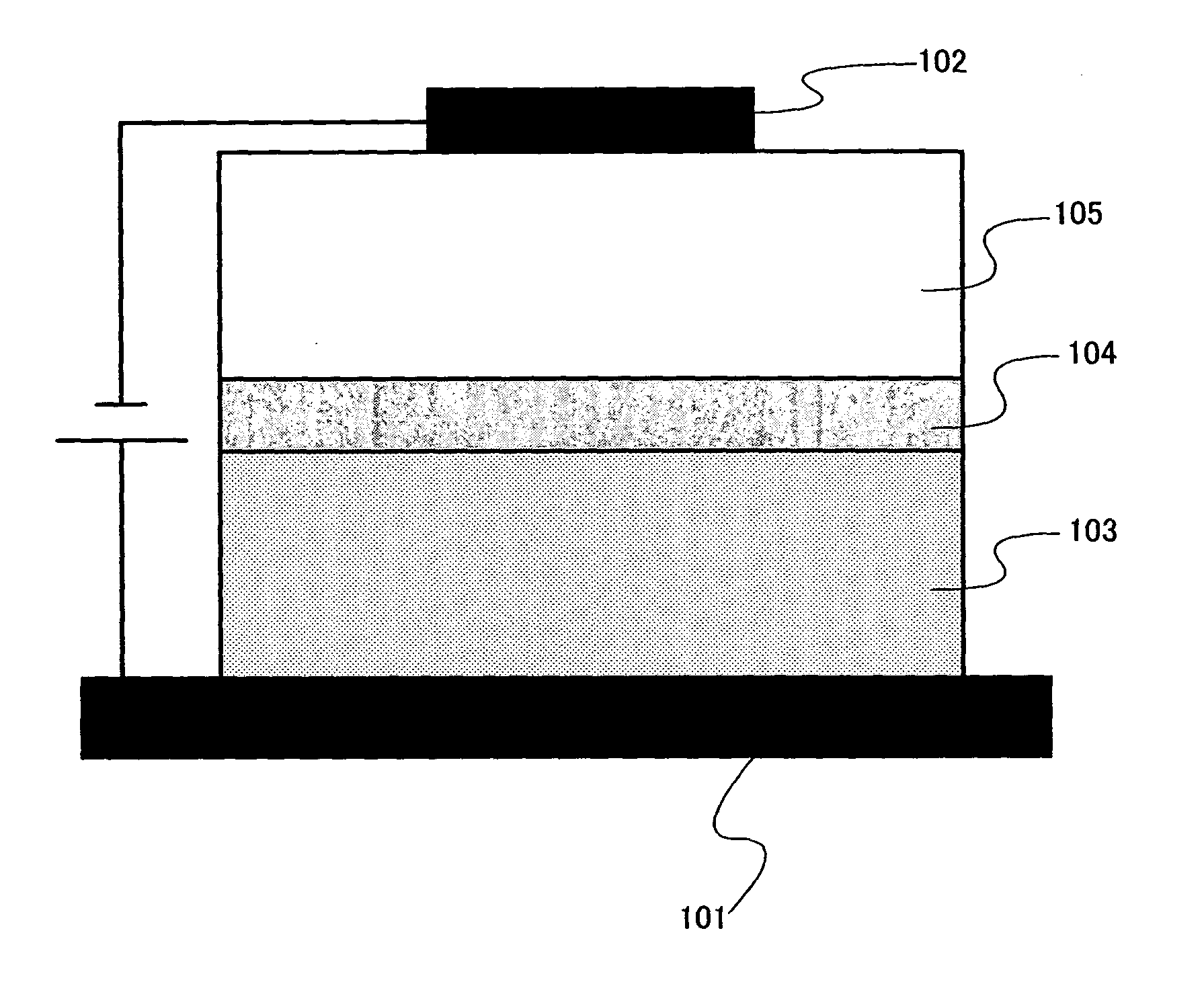
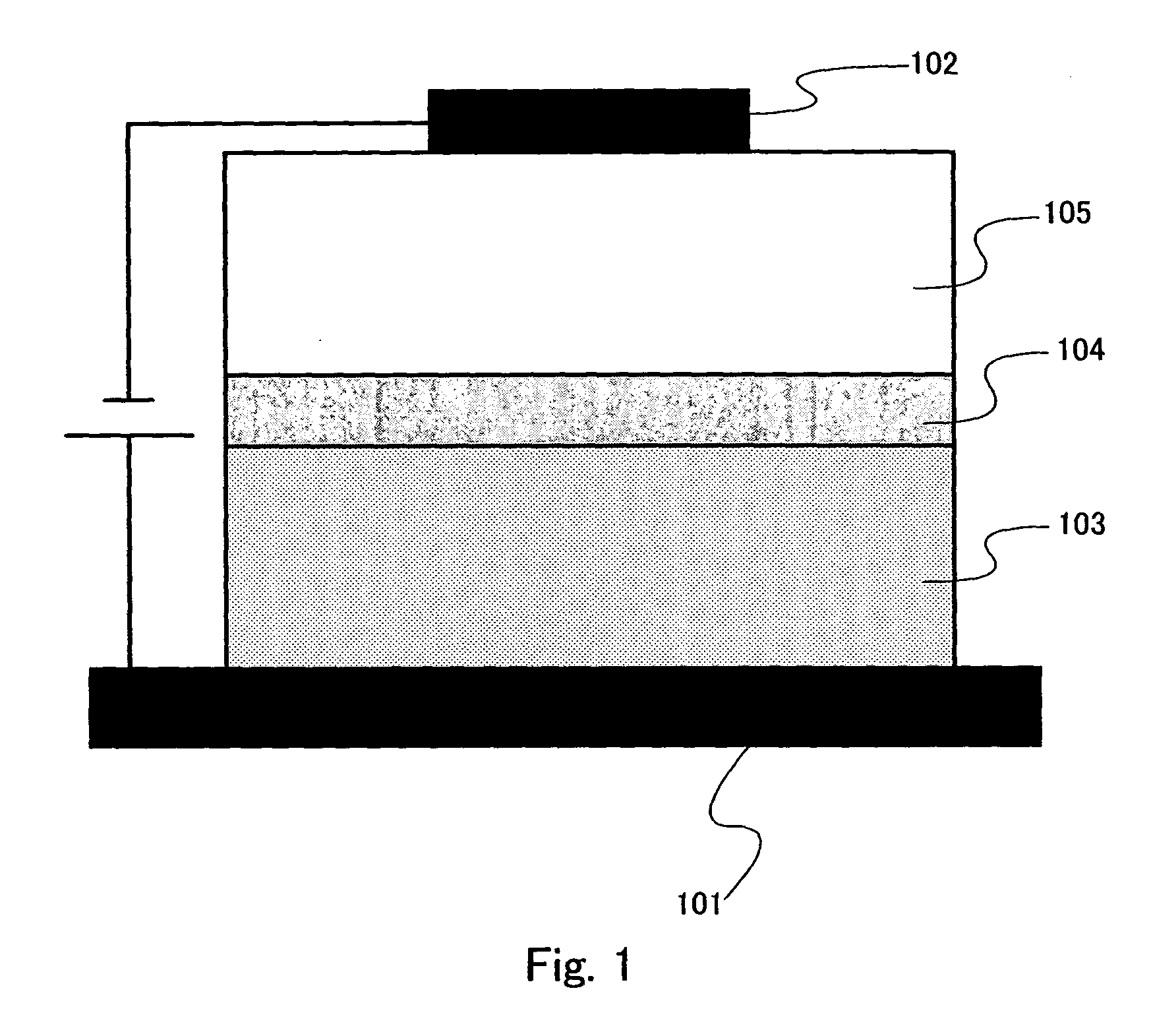
[0118] In this embodiment, an EL element according to the present invention shown in FIG. 1 will be specifically described. This embodiment will be described two examples that an EL element according to the present invention in which a hole blocking material is introduced into an electroluminescent film (hereinafter, an element D) and an EL element according to the present invention in which a hole blocking material is introduced into an electron transport supporting layer (hereinafter, an element E).

[0119] The structure of the device D is "ITO (110 nm), CuPc (20 nm), .alpha.-NPD (30 nm), Alq (40 nm), BCP (10 nm), CaF.sub.2 (2 nm), Al (20 nm), Au (20 nm), Alq (100 nm), CaF.sub.2 (2 nm), Al (100 nm)". The structure of the device E is "ITO (110 nm), CuPc (20 nm), .alpha.-NPD (30 nm), Alq (50 nm), CaF.sub.2 (2 nm), Al (20 nm), BCP (100 nm), Al (100 nm)". Hole blocking materials for the device D and device E are BCP. In addition, in either device, the size of the pixel is 2-nm-square.

[0...

embodiment 3

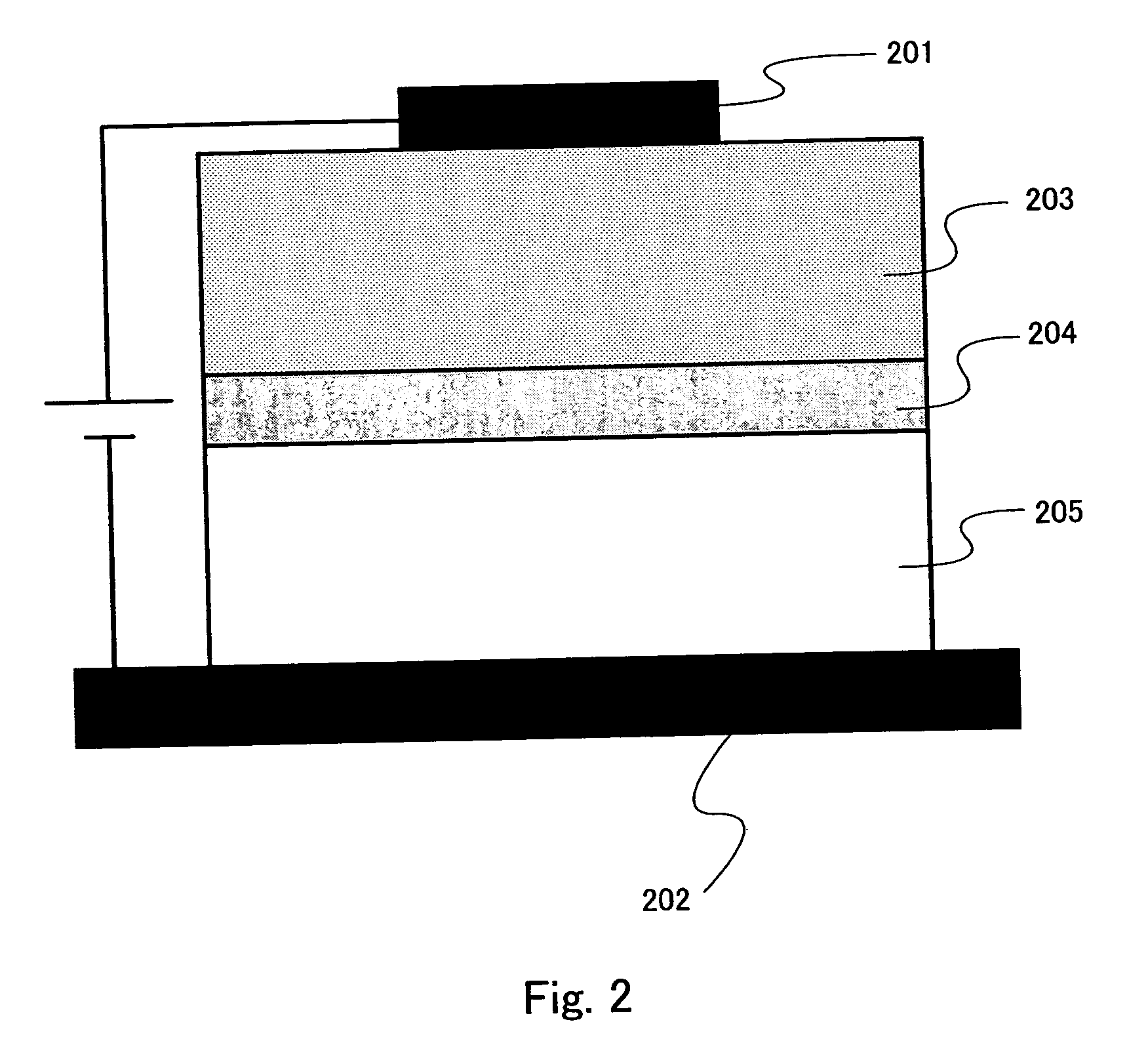
[0123] An EL element shown in FIG. 2 will be specifically described in this embodiment.

[0124] Basically, the device shown in FIG. 2 can be fabricated through the reverse process to that of FIG. 1. First, BCP is deposited to have a thickness of 100 nm as an electron transport supporting layer on the substrate on which Al is deposited to have a thickness of 100 nm as a cathode 202, and Al: Li alloy is deposited to have a thickness of 20 nm as a floating electrode 204 thereon.

[0125] Next, Alq as an electron transporting luminescent material is deposited to have a thickness of 50 nm, .alpha.-NPD as a hole transporting material is deposited to have a thickness of 30 nm, and CuPc as a hole injecting material is deposited to have a thickness of 20 nm in this order to form an electroluminescent film 203. Lastly, Au is deposited to have a thickness of 20 nm as an anode 201, and an EL element according to the present invention can be obtained. Light is extracted from the top surface (Au side)...


PUM


Abstract

An EL element which is thicker and lower-voltage drive without doping acceptor or donor than the conventional one. An EL element in which an electroluminescent film 103 containing an organic compound which can provide electroluminescent, a floating electrode 104, an electron transport supporting layer 105 and a cathode 102 are in order laminated on an anode 101. A film thickness of the electroluminescent film 103 is on the order of a conventional film thickness (on the order of approximately 100 nm), and the electron transport supporting layer 105 may also have a film thickness on the order of the electroluminescent film 103. The EL element can be driven at lower voltage than the conventional one by introducing a hole blocking material into an electron transport supporting layer.

Description

[0001] 1. Field of the Invention[0002] The present invention relates to an electroluminescent device (hereinafter, an EL element) having a film comprising an organic compound (hereinafter, an electroluminescent film) that emits light by applying an electronic field, an anode, and a cathode. More particularly, the present invention relates to an EL element that has good yields, high reliability, and low-voltage drive; and a light emitting device that includes the EL element. A light emitting device in this specification includes an image display device including an EL element, and also module in which a connector, a flexible printed circuit board (FPC), TAB (tape automated bonding), or TAB (tape carrier package) are attached to an EL element, or module in which a print circuit plate is attached to a tip of the TAB or TCP, or module in which IC (integrated circuit) is mounted directly on an EL element by COG (Chip On Glass).[0003] 2. Description of the Related Art[0004] The EL element...

Claims


Application Information

Patent Timeline
Patent Type & Authority Applications(United States)
IPC IPC(8): H01L27/32H05B33/26H01L51/00H01L51/30H01L51/50H01L51/52
CPCH01L27/3244H01L51/0059H01L51/0078H01L2251/558H01L51/5096H01L51/5203H01L2251/5315H01L51/0081H10K59/12H10K85/631H10K85/311H10K85/324H10K50/18H10K50/805H10K2102/3026H10K2102/351H05B33/26
Inventor SEO, SATOSHIYAMAZAKI, HIROKO
Owner SEMICON ENERGY LAB CO LTD
Why Eureka
Try Eureka