Semiconductor device including metal insulator semiconductor field effect transistor and method of manufacturing the same

a semiconductor field effect transistor and semiconductor technology, applied in the direction of semiconductor devices, electrical devices, transistors, etc., can solve the problems of difficult control of each threshold voltage to a proper value on circuit operation, unwanted chemical reaction at the substrate surface, inferior heat resistance of materials to polysilicon

Inactive Publication Date: 2004-05-06
KIOXIA CORP
View PDF9 Cites 38 Cited by
  • Summary
  • Abstract
  • Description
  • Claims
  • Application Information

AI Technical Summary

Benefits of technology

[0040] A dummy gate structure, which is removed in a post-process, is formed. That is, the silicon oxide film having a thickness of, e.g. 6 nm is formed by thermal oxidation. A P-type impurity is introduced by an ion implantation method in order to control a threshold voltage of the N-channel MISFET. Subsequently, a polysilicon film having the thickness of, e.g. about 100 nm is deposited by CVD method, and a silicon nitride film having the thickness of, e.g. 20 nm is formed. These films are patterned by a lithography method, dry etching, or the like to provide an insulating film 103, a conductive film 104, and a first cap film 105, which become the dummy gate structure. Extension regions 106 and 107 are formed by the ion implantation using the first cap film 105, the conductive film 104, and the isolation film 103, which are patterned, as a mask. That is, arsenic ions or phosphorus ions are implanted at the dose of 1.times.10.sup.13 cm.sup.-2 to 5.times.10.sup.15 cm.sup.2, and then the doped impurity is activated by, e.g. rapid heating for several seconds. The extension regions 106 and 107 may be formed by the ion implantation without patterning the insulating film 103 and then the insulating film 103 may be patterned.

Problems solved by technology

However, these materials have a drawback that the materials are inferior in heat resistance to polysilicon.
In the case that the above-described method is applied to the integrated circuit including the complementary circuit, work functions of the gate electrodes become the same when the same metals are used for the gate electrodes of an N-channel MISFET and a P-channel MISFET, so that it becomes difficult to control each threshold voltage to a proper value on circuit operation.
Therefore, in the process in which the first gate electrode material is removed by the etching, the gate insulating film of the P-channel MISFET is always exposed to etching species such as a gas or chemicals, whereby unwanted chemical reaction occurs at the substrate surface.
Further, even in the subsequent cleaning processes, the similar reaction is caused by the chemicals for removing metal contamination and the like.
Accordingly, in the case that the gate insulating film is exposed to the gas or chemicals, even if the etching species is selected so that the etching of the gate insulating film is not generated in a macroscopic level, there occurs a problem that uniformity of the gate insulating film is degraded in a microscopic level.
The above-described non-uniformity would become the large problem because it acts as a factor for providing an adverse effect and variation to the reliability.

Method used


Image

  • Semiconductor device including metal insulator semiconductor field effect transistor and method of manufacturing the same
  • Semiconductor device including metal insulator semiconductor field effect transistor and method of manufacturing the same
  • Semiconductor device including metal insulator semiconductor field effect transistor and method of manufacturing the same

Examples


first embodiment

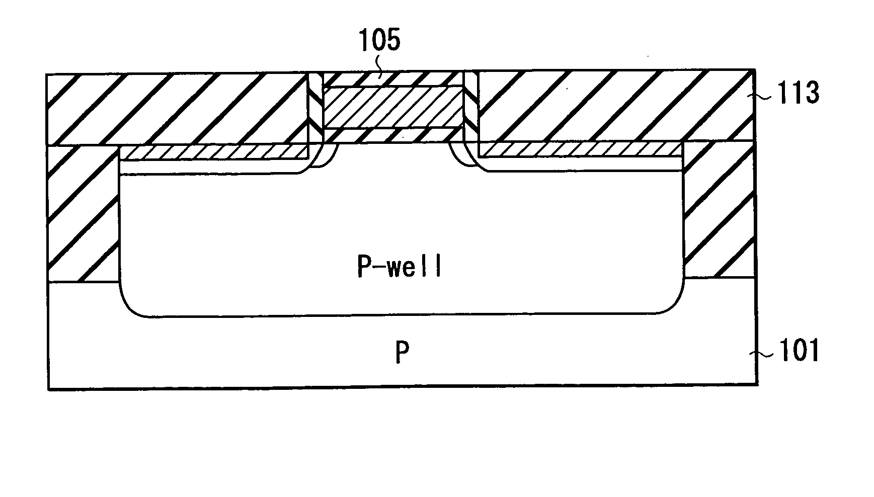
[0063] Since the work function of tungsten silicide is increased as the silicon content of tungsten silicide is decreased, even when the gate electrode of the P-channel MISFET includes the third metal silicide, the work function of the gate electrode of the P-channel MISFET has the value larger than that of the work function of the gate electrode of the N-channel MISFET. Therefore, the gate electrode shown in the above-described first embodiment becomes the optimum structure as the complementary circuit constituting the integrated circuit.

[0064] For the above-described reasons, it is desirable that the number of silicon atoms per unit volume is 2.5 times not lower than the number of metal atoms per unit volume in the composition ratio between silicon and metal constituting the first metal silicide 115 which is the gate electrode of the N-channel MISFET. Further, it is desirable that the number of silicon atoms per unit volume is not more than the number of metal atoms per unit volum...

second embodiment

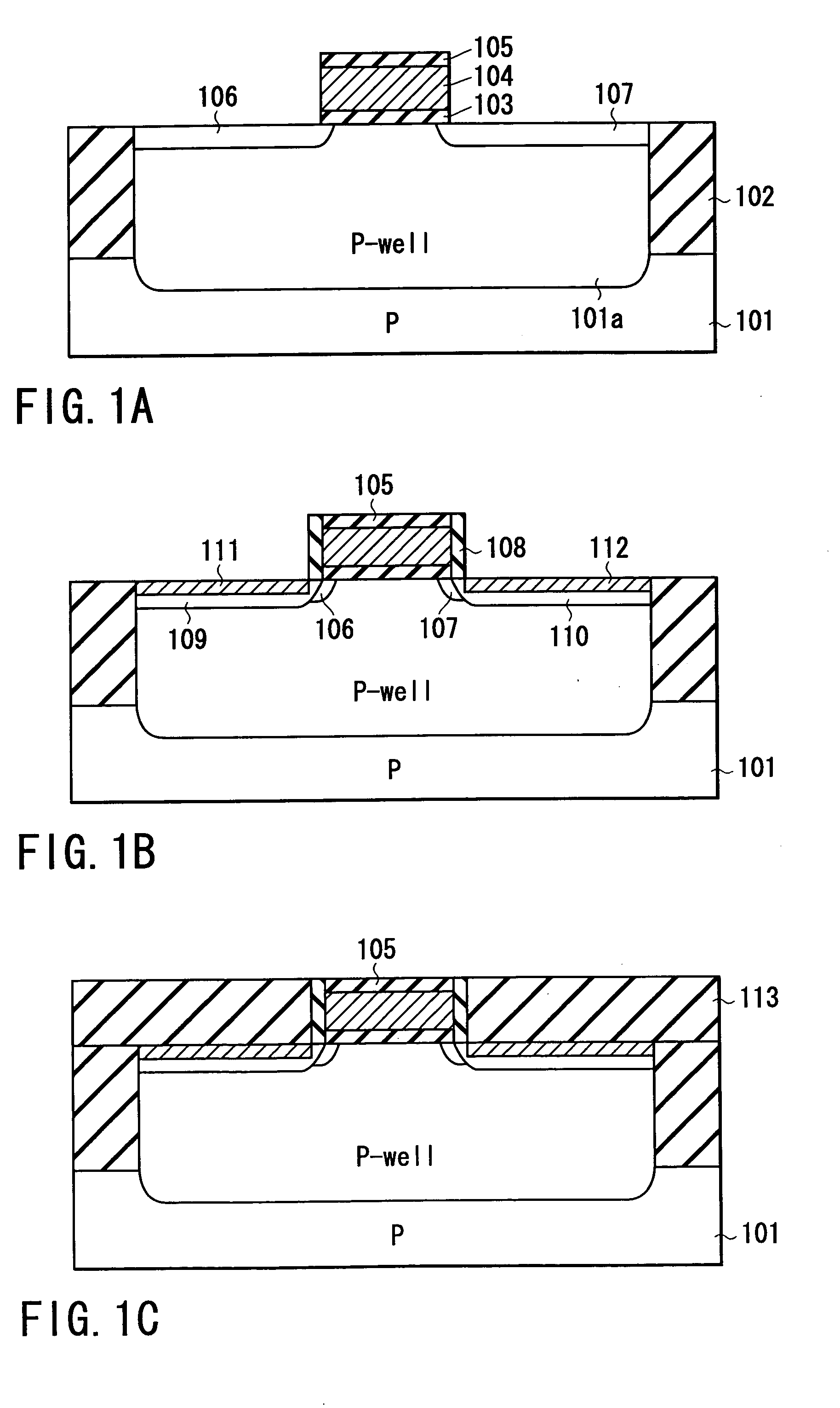
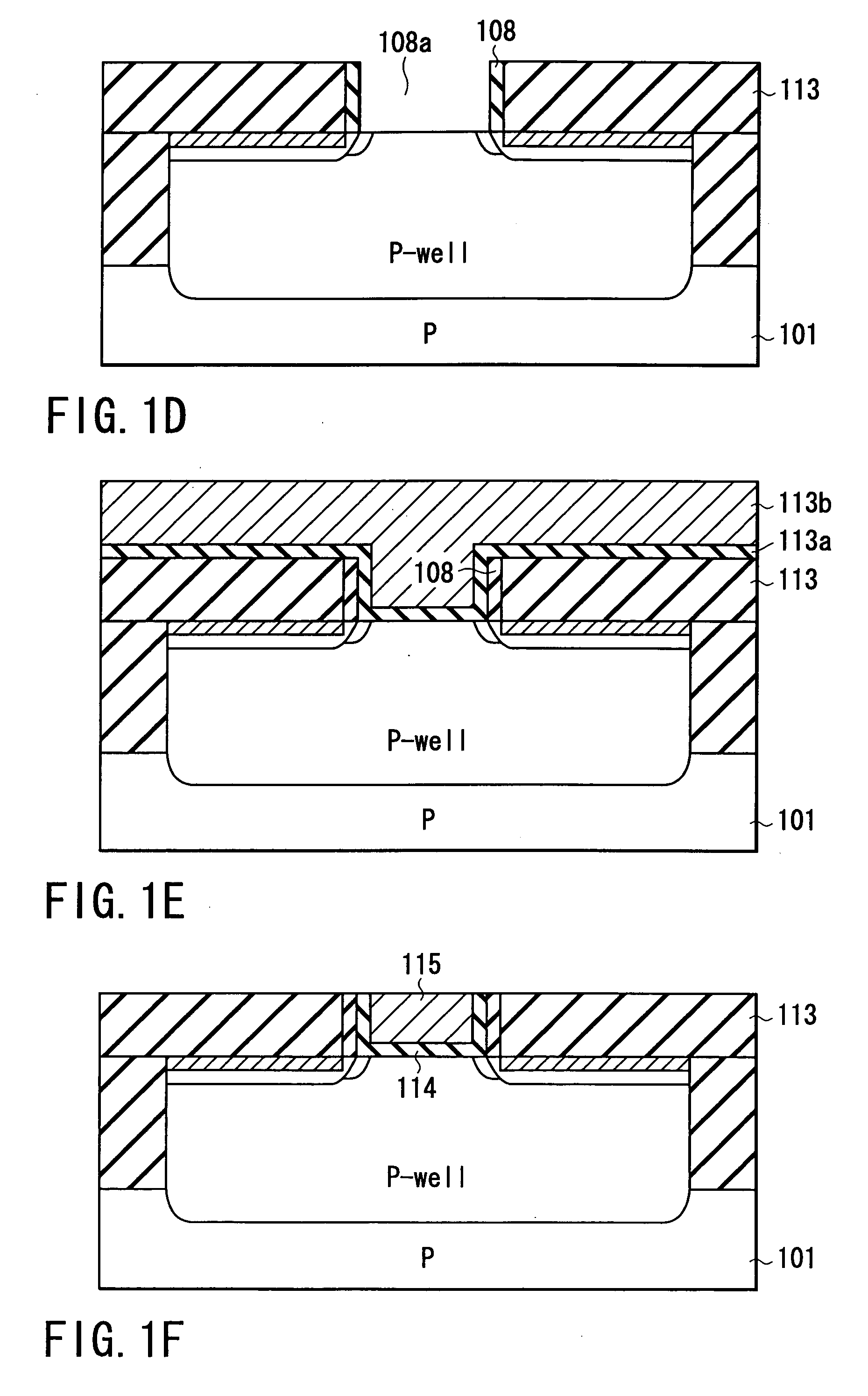
[0066] A method of manufacturing a semiconductor device including MISFETs will be described referring to FIGS. 3A to 3K.

[0067] Though both the N-channel MISFET and the P-channel MISFET are formed in the second embodiment, only the region of the N-channel MISFET is typically shown in the steps of FIGS. 3A to 3E. The steps from FIG. 3F are shown for both the N-channel MISFET and the P-channel MISFET.

[0068] The manufacturing method of the embodiment is characterized in that the metal silicide electrode layer is formed on the upper surface of the source and drain regions after the film formation of the gate insulating film and the gate electrode is carried out.

[0069] As shown in FIG. 3A, an oxide film is selectively formed in a P-type silicon substrate 201 by STI (shallow trench isolation) process or LOCOS (local oxidation of silicon) process to provide an isolation region 202 therein. Boron ions are implanted at a dose of 1.times.10.sup.12 cm.sup.-2 to 1.times.10.sup.14 cm.sup.-2 usin...

third embodiment

[0085] A method of manufacturing a semiconductor device including MISFETs will be described referring to FIGS. 4A to 4H.

[0086] Though both the N-channel MISFET and the P-channel MISFET are also formed in the third embodiment, only the region of the N-channel MISFET is typically shown in the steps of FIGS. 4A to 4C. The steps from FIG. 4D are shown for both the N-channel MISFET and the P-channel MISFET.

[0087] In the embodiment, the silicon film for the source and drain regions is selectively grown on the silicon substrate surface to form elevated source and drain regions.

[0088] As shown in FIG. 4A, an isolation region 302 is formed in a P-type silicon substrate 301 in a manner so as to selectively form an oxide film by STI (shallow trench isolation) process or LOCOS (local oxidation of silicon) process. Boron ions are implanted at the dose of 1.times.10.sup.12 cm.sup.-2 to 1.times.10.sup.14 cm.sup.-2 using the ion implantation. Then, the doped impurity is activated by, e.g. rapid he...


PUM


Abstract

A semiconductor device comprises a semiconductor substrate, an N-channel MISFET and a P-channel MISFET provided on the semiconductor substrate, each of the N- and P-channel MISFETs being isolated by an isolation region and having a gate insulating film, a first gate electrode film provided on the gate insulating film of the N-channel MISFET and composed of a first metal silicide, a second gate electrode film provided on the gate insulating film of the P-channel MISFET and composed of a second metal silicide made of a second metal material different from a first metal material composing the first metal silicide, and a work function of the first gate electrode film being lower than that of the second gate electrode film.

Description

[0001] This application is based upon and claims the benefit of priority from the prior Japanese Patent Application No. 2002-322094, filed Nov. 6, 2002, the entire contents of which are incorporated herein by reference.[0002] 1. Field of the Invention[0003] The present invention relates to a semiconductor device including insulated gate field effect transistors (hereinafter referred to as MISFET) and a method of manufacturing the same.[0004] 2. Description of the Related Art[0005] An integrated circuit having high performance is demanded, and high-speed operation is also demanded for a complementary circuit which is one of basic circuits. For the high-speed operation of the complementary circuit, a method in which a channel length of MISFET being a basic element of the complementary circuit is decreased by a fine device technique has been used. Since the fine device structure involves formation of thin films for a gate insulating film and a gate electrode film of MISFET, corresponde...

Claims


Application Information

Patent Timeline
Patent Type & Authority Applications(United States)
IPC IPC(8): H01L21/28H01L21/336H01L21/8238H01L27/092H01L29/423H01L29/49H01L29/78H01L29/786
CPCH01L21/28097H01L21/823814H01L29/66545H01L21/823864H01L21/823842
Inventor MATSUO, KOUJI
Owner KIOXIA CORP
Why Eureka
Try Eureka