

Semiconductor crystal film and method for preparation thereof
Image

Examples
first embodiment
[0064] FIG. 5 is a diagram showing a composition range in which a single crystal can be produced with a known single-layer SiGeC layer and a composition range for a multi-layer film serving as a SiGeC layer that can be produced according to the present invention. As shown in FIG. 5, the alternate deposition of the Si.sub.0.2Ge.sub.0.8 and Si.sub.0.785Ge.sub.0.2C.sub.0.015 layers 12 and 13 results in a multi-layer film serving as a SiGeC layer whose compositional percentages are indicated by any one point corresponding to the ratio of the thickness of the Si.sub.0.2Ge.sub.0.8 layer 12 to that of the Si.sub.0.785Ge.sub.0.2C.sub.0.015 layer 13 on the line L1. For example, if the thickness ratio of the Si.sub.0.2Ge.sub.0.8 layer 12 to the Si.sub.0.785Ge.sub.0.2C.sub.0.015 layer 13 is 1:1.5, the resultant multi-layer film 10B (of the modified example of the first embodiment) serves as a SiGeC layer with a composition on the point P15 shown in FIG. 5.
[0065] If a Si.sub.1-x1-y1Ge.sub.x1C.s...
embodiment 2
[0070] In the first embodiment, the inventive multi-layer film, which is obtained by alternate epitaxial growths of two crystal films having two mutually different compositions, and the method for producing the film have been described. In this embodiment, another inventive multi-layer film that is obtained by alternate epitaxial growths of three crystal layers having mutually different compositions will be described.
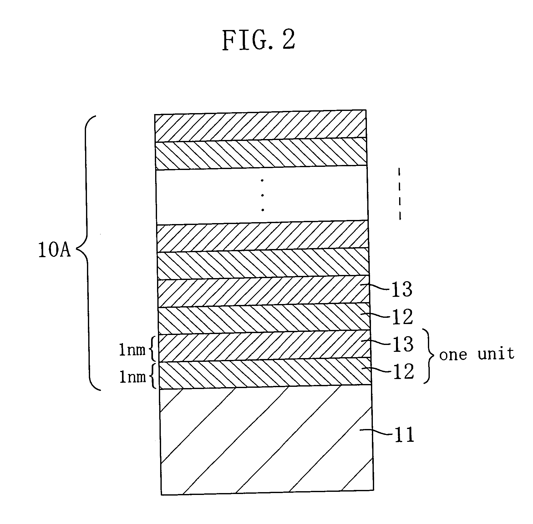
[0071] FIG. 6 is a cross-sectional view schematically showing a structure of a multi-layer film (a semiconductor crystal film) according to a second embodiment of the present invention. In this embodiment, a Si.sub.0.2Ge.sub.0.8 layer 12 with a thickness of about 1 nm having a larger lattice constant than Si crystal and a Si.sub.0.785Ge.sub.0.2C.sub-.0.015 layer 13 with a thickness of about 1 nm, and a Si.sub.0.832Ge.sub.0.15C.sub.0.018 layer 14 with a thickness of about 1 nm are alternately deposited on a Si substrate 11 a plurality of times (33 cycles in this embodime...
embodiment 3
[0079] Next, an example of a hetero bipolar transistor with the multi-layer film 10A, 10B or 10C serving as a SiGeC film described in the foregoing embodiments.
[0080] FIG. 7 is a cross-sectional view schematically showing a structure of an npn heterojunction bipolar transistor (HBT) according to this embodiment. As shown in FIG. 7, the HBT of this embodiment includes: an n.sup.+ layer 31, which is defined in a Si substrate 30 and contains an n-type dopant (e.g., phosphorus) at a high-concentration; a collector layer 33, which is epitaxially grown on the n.sup.+ layer 31 and contains an n-type dopant (e.g., phosphorus) at a low-concentration; an isolation layer 32 of a thermal oxide film, which defines the collector layer 33; a first deposited oxide film 35 formed on the isolation layer 32; a multi-layer film 36, which fills in an opening (an opening for base) formed in the isolation layer 32 and the first deposited oxide film 35 to extend over the first deposited oxide film 35 and w...
PUM
 Abstract
Description
Claims
Application Information
- IPC
- H01L21/205; H01L29/15; H01L29/24; H01L29/737; H01L29/80
- CPC
- H01L29/155; H01L29/1608; H01L29/7378; H01L29/802; H01L21/02507; H01L21/02381; H01L21/02661; H01L21/0245
- Inventors
- KANZAWA, YOSHIHIKO; SAITOH, TOHRU