Check patentability & draft patents in minutes with Patsnap Eureka AI!

Semiconductor laser comprising a plurality of optically active regions

Inactive Publication Date: 2004-06-24
UNIV OF GLASGOW THE UNIV COURT OF
View PDF3 Cites 10 Cited by
  • Summary
  • Abstract
  • Description
  • Claims
  • Application Information

AI Technical Summary

Benefits of technology

0052] FIG. 1 a simplified schematic perspective view from one side to one end and above

Problems solved by technology

Broad area lasers are used for high power applications, but suffer from a number of problems such as filamentation, instabilities in the transverse mode, and poor far-field characteristics.

Method used


Image

  • Semiconductor laser comprising a plurality of optically active regions
  • Semiconductor laser comprising a plurality of optically active regions
  • Semiconductor laser comprising a plurality of optically active regions

Examples


Embodiment Construction

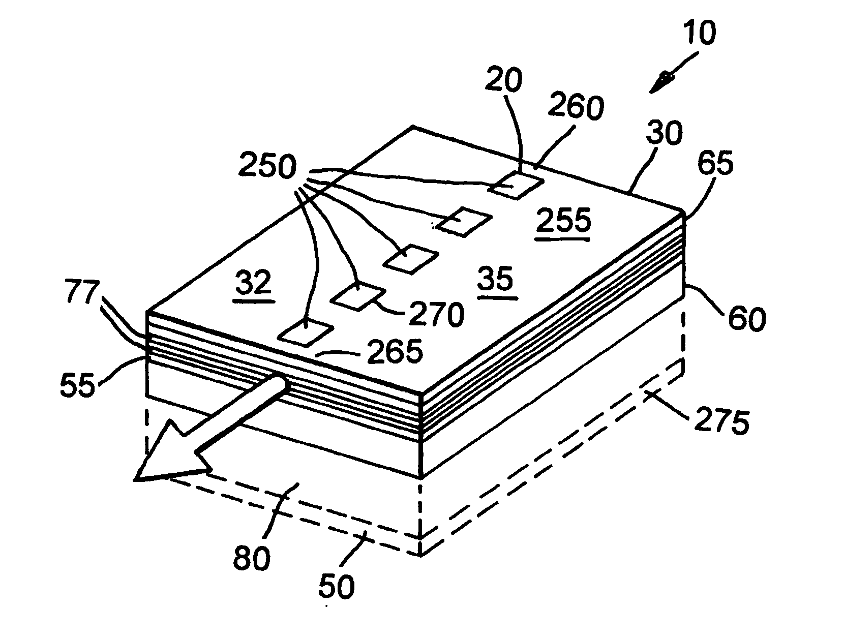
[0081] As an example of improved device performance, a second embodiment of a segmented gain section laser device according to the present invention fabricated in the InGaAsP / GaAs material system will now be given.

[0082] The wafer structure used was a 670 nm double Quantum Well (QW) laser layer, grown on a (100) Si doped GaAs substrate misoriented 10.degree. to the (111) A direction. The misoriented wafer ensured that ordering of the AlGaInP quaternary was minimised securing good laser performance. The epitaxial layer structure is listed in Table 1. The lasing spectrum was centred on 676 nm with a turn on voltage of 1.987V. A typical threshold current density for infinite cavity length was 330 A cm.sup.-2.

1TABLE 1 Carrier concentration Layer Material Thickness Purpose Dopant (cm.sup.-3) Number GaAs 300 nm Cap Zn 8 .times. 10.sup.18 --Ga.sub.0.5In.sub.0.5P 20 nm Grading Zn 2 .times. 10.sup.18 --Layer (Al.sub.0.7Ga.sub.0.3).sub.0.5 1000 nm Upper Zn 8 .times. 10.sup.17 65 In.sub.0.5P c...


PUM


Abstract

There is disclosed an improved semiconductor laser device (10), and particularly, a broad area semiconductor laser with a singe-lobed far field pattern. Known broad area lasers are used for high power applications, but suffer from a number of problems such as filamentation, instabilities in the transverse mode, and poor far-field characteristics. The present invention addresses such by providing a semiconductor laser device (10) comprising: a plurality of optically active regions (240); each optically active region (240) including a Quantum Well (QW) structure (77); adjacent optically active regions (24) being spaced by an optically passive region; the / each optically passive region (245) being Quantum Well Intermixed (QW). The spacing between adjacent optically active regions (240) may conveniently be termed "segmentation".

Description

[0001] The present invention relates to semiconductor laser devices, and in particular, though not exclusively, to a broad area semiconductor laser with a single-lobed far field pattern.[0002] The present application is related to pending Application Number GB 01 01 641.9 of Jan. 23, 2001, also by the same Applicant and entitled "Improvements in or Relating to Semiconductor Lasers".BACKGROUND TO INVENTION[0003] Broad area lasers are used for high power applications, but suffer from a number of problems such as filamentation, instabilities in the transverse mode, and poor far-field characteristics. A reason for filament formation is related to the self-focusing nonlinear behaviour that occurs in the gain section of a broad stripe semiconductor laser.[0004] An object of the present invention is to obviate or mitigate the aforementioned problems in the prior art.[0005] A further object of the present invention is to provide a broad area semiconductor laser that exhibits a high power ou...

Claims


Application Information

Patent Timeline
IPC IPC(8): H01S5/042H01S5/0625H01S5/068H01S5/11H01S5/20H01S5/34
CPCB82Y20/00H01S5/0425H01S5/10H01S5/1057H01S2301/18H01S5/1225H01S5/1228H01S5/2036H01S5/3413H01S5/12H01S5/04254H01S5/11
Inventor MARSH, JOHN HAIGKIM, SHIN-SUNG
Owner UNIV OF GLASGOW THE UNIV COURT OF
Features
  • R&D
  • Intellectual Property
  • Life Sciences
  • Materials
  • Tech Scout
  • Unparalleled Data Quality
  • Higher Quality Content
  • 60% Fewer Hallucinations
Learn More