Laser-based method and system for memory link processing with picosecond lasers

a memory link and laser technology, applied in the direction of conductors, semiconductor/solid-state device testing/measurement, semiconductor/solid-state device details, etc., can solve the problems of high pressure build-up of molten link contained by oxide, small device, and low thickness of interconnects and links. achieve the effect of improving the quality of laser processing

Inactive Publication Date: 2004-07-15
ELECTRO SCI IND INC
View PDF99 Cites 112 Cited by
  • Summary
  • Abstract
  • Description
  • Claims
  • Application Information

AI Technical Summary

Benefits of technology

[0012] An object of the present invention is to provide a method or apparatus for improving the quality of laser processing (i.e., removal, ablation, severing, "blowing," etc.) of memory links.

Problems solved by technology

Not only are the devices small, but the interconnects and links thickness have also decreased dramatically in recent years.
The differential expansion results in a high pressure build-up of the molten link contained by the oxide.
If the pressure is too low, the link will not be removed cleanly.
Current commercial laser memory link repair systems, which use Q-switched, Nd based solid-state lasers with wavelengths of about 1 to 1.3 microns and pulse widths about 4 to 50 nanoseconds (ns), are not well suited for meeting such requirements.
In summary, the conventional q-switched, nanosecond solid state lasers, even at short wavelengths, are not able to process the fine pitch links due to its thermal process nature.
Material interaction may be a substantially non-thermal process at femtosecond pulse widths, but the complexity, high costs, and reliability of femtosecond pulse lasers may limit practical implementations.
Device and material modifications to support laser repair are expensive and alone may not be sufficient.

Method used


Image

  • Laser-based method and system for memory link processing with picosecond lasers
  • Laser-based method and system for memory link processing with picosecond lasers
  • Laser-based method and system for memory link processing with picosecond lasers

Examples


Embodiment Construction

)

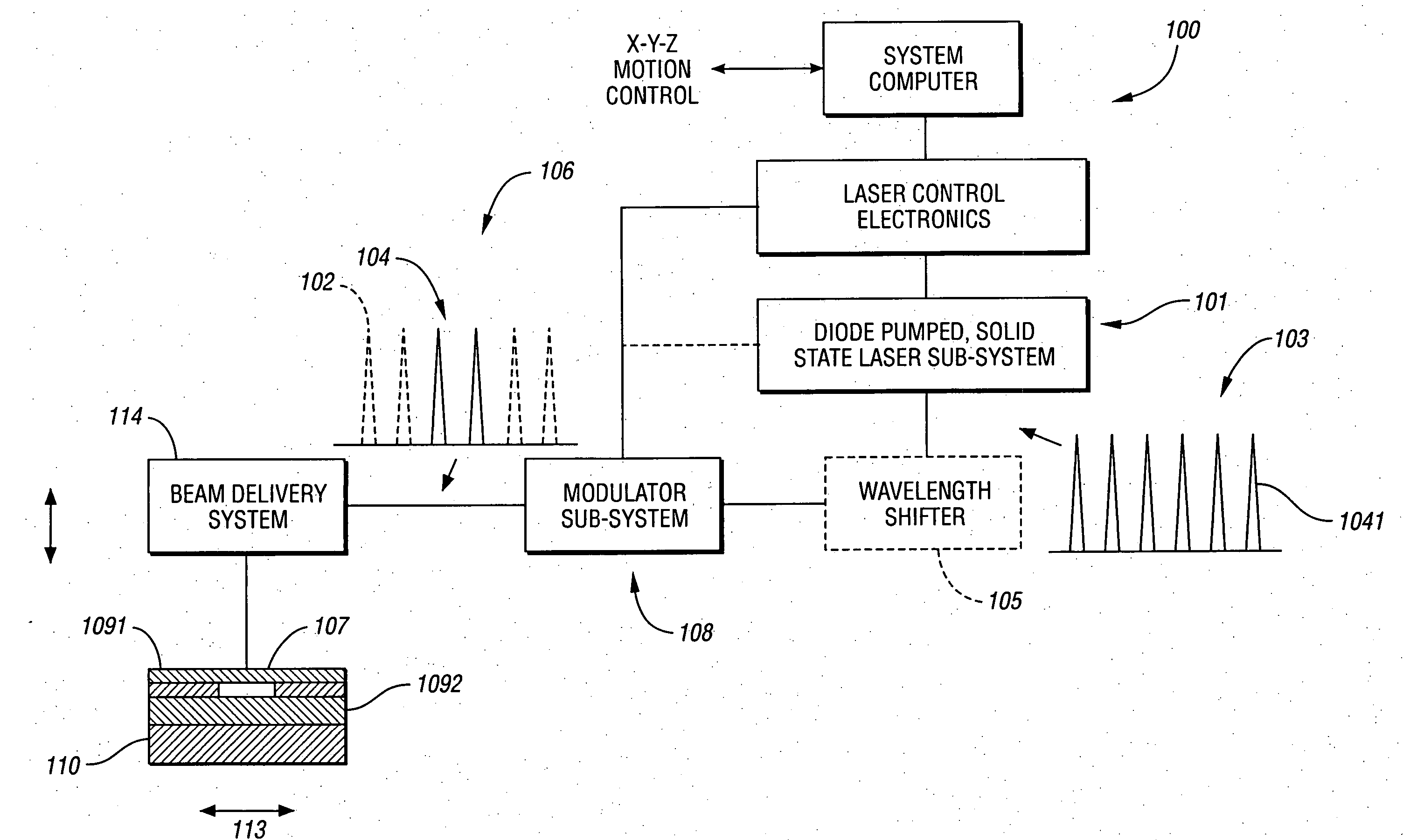
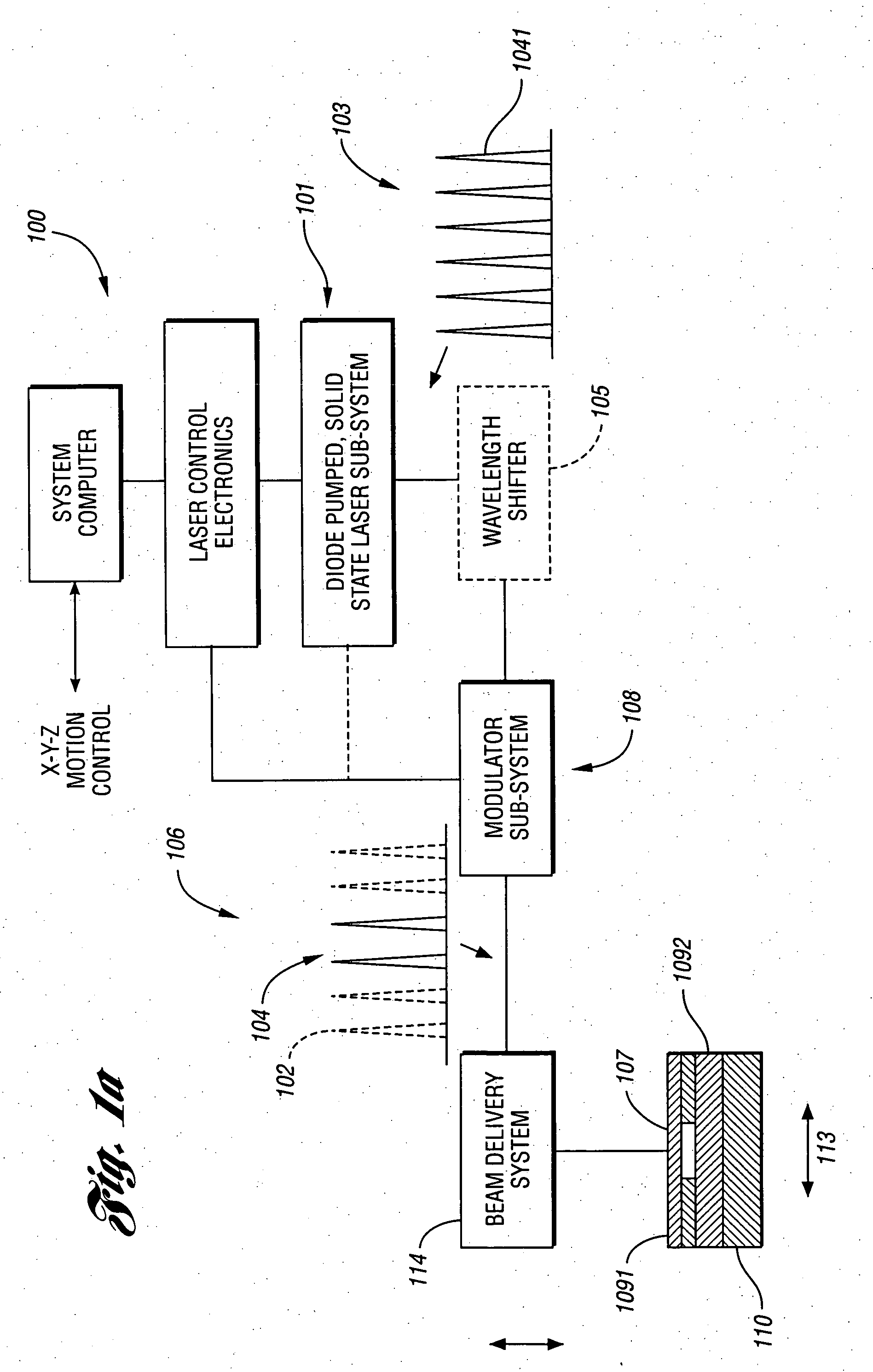
[0092] Overview--Laser System Architecture

[0093] Referring to FIG. 1a, a block diagram illustrating a portion of a laser processing system 100 for removal of an electrically conductive link 107 using at least one output pulse 104 having a picosecond pulse width (i.e., pulse duration, etc.) 1041 (e.g., as measured at the half power point) and shows some major system components included in at least one embodiment of the present invention is shown. At least one embodiment of the invention may include a diode pumped, solid state laser in sub-system 101 to produce intermediate pulses 103 having pulse widths 1041 in a preferred picosecond range. The laser may be a commercially available diode pumped, solid state (active or passive) mode locked laser, for instance. For operation at a preferred wavelength the output 103 of the system 101 may be shifted in wavelength by optional shifter 105 (e.g., a harmonic generator) for example from a near infrared wavelength to a visible or near UV wave...


PUM

PropertyMeasurementUnit
wavelengthaaaaaaaaaa
pre-determined wavelengthaaaaaaaaaa

Abstract

A laser-based method of removing a target link structure of a circuit fabricated on a substrate includes generating a pulsed laser output at a pre-determined wavelength less than an absorption edge of the substrate. The laser output includes at least one pulse having a pulse duration in the range of about 10 picoseconds to less than 1 nanosecond, the pulse duration being within a thermal laser processing range. The method also includes delivering and focusing the laser output onto the target link structure. The focused laser output has sufficient power density at a location within the target structure to reduce the reflectivity of the target structure and efficiently couple the focused laser output into the target structure to remove the link without damaging the substrate.

Description

[0001] This application is a continuation in part of U.S. Ser. No. 09 / 941,389 entitled "Energy-Efficient, Laser Based Method and System for Processing Target Material", filed 28 Aug. 2001, which is a continuation of U.S. Ser. No. 09 / 473,926, filed 28 Dec. 1999, now U.S. Pat. No. 6,281,471. The disclosure of U.S. Pat. No. 6,281,471 is hereby incorporated by reference in its entirety. This application is also a continuation in part of U.S. Ser. No. 10 / 107,890 entitled "Methods and Systems for Thermal-Based Laser Processing a Multi-Material Device" filed 27 Mar. 2002, which claims the benefit of U.S. Provisional Application Ser. No. 60 / 279,644, filed 29 Mar. 2001. The disclosure of U.S. Ser. No. 10 / 107,890, now published as U.S. Patent Application Publication Number 2002 / 0167581, is hereby incorporated by reference in its entirety.[0002] 1. Field of the Invention[0003] The present invention relates to the field of laser processing methods and systems, and specifically, to laser process...

Claims


Application Information

Patent Timeline
Patent Type & Authority Applications(United States)
IPC IPC(8): B23K26/00B23K26/04B23K26/06B23K26/073B23K26/36B23K26/38B23K26/40H01L21/48H01L21/66H01L21/768H01L23/525H01SH05K3/00
CPCB23K26/04H05K3/0026B23K26/0736B23K26/365B23K26/386B23K26/40B23K26/401B23K26/402B23K2201/38B23K2201/40B23K2203/08B23K2203/10B23K2203/12H01L21/485H01L21/76894H01L22/12H01L23/5258B23K26/0635B23K26/0624B23K26/361B23K26/389B23K2101/38B23K2101/40B23K2103/08B23K2103/10B23K2103/12B23K2103/50H01L2924/0002H01L2924/00
Inventor GU, BOSMART, DONALD V.CORDINGLEY, JAMES J.LEE, JOOHANSVETKOFF, DONALD J.JOHNSON, SHEPARD D.EHRMANN, JONATHAN S.
Owner ELECTRO SCI IND INC
Why Eureka
Try Eureka