Circuit component built-in module with embedded semiconductor chip and method of manufacturing

a semiconductor chip and built-in module technology, applied in the association of printed circuit non-printed electric components, basic electric elements, solid-state devices, etc., can solve the problems of reducing manufacturing yield, reducing manufacturing yield, and high cost of substrate recess formation process

Inactive Publication Date: 2004-07-29
PANASONIC CORP
View PDF33 Cites 229 Cited by
  • Summary
  • Abstract
  • Description
  • Claims
  • Application Information

AI Technical Summary

Problems solved by technology

Since a conventional technique in which a through hole structure is formed by drilling a substrate that is formed by impregnating a glass fiber cloth with an epoxy resin (glass-epoxy substrate) has a limited capability for achieving the high densification, there arises a problem that connections of wiring patterns between large scale integrated circuits (LSI) and between components cannot be achieved with minimum distances.
However, when the technique of providing the recessed space 1010 in the circuit substrate and arranging the semiconductor chip 1001 therein is used, the process of forming a recess in the substrate is expensive, irrespective of which type is used, a ceramic substrate or a resin-based substrate, and a problem of a decrease in the manufacturing yield arises also.
In this case, since the material used for forming a substrate normally is a resin such as glass-epoxy, the thermal conductivity of the substrate itself is low, thereby causing a module obtained to have a limited heat dissipating property, and impairing the reliability.
Furthermore, in a circuit component built-in module having multiple layers of circuit substrates, in a case where a multiplicity of circuit substrates are stacked in a vertical direction, the high-density mounting is limited, since the module as a whole has a relatively great thickness.
In the case of a memory module in which memory semiconductor chips of d

Method used


Image

  • Circuit component built-in module with embedded semiconductor chip and method of manufacturing
  • Circuit component built-in module with embedded semiconductor chip and method of manufacturing
  • Circuit component built-in module with embedded semiconductor chip and method of manufacturing

Examples


embodiment 2

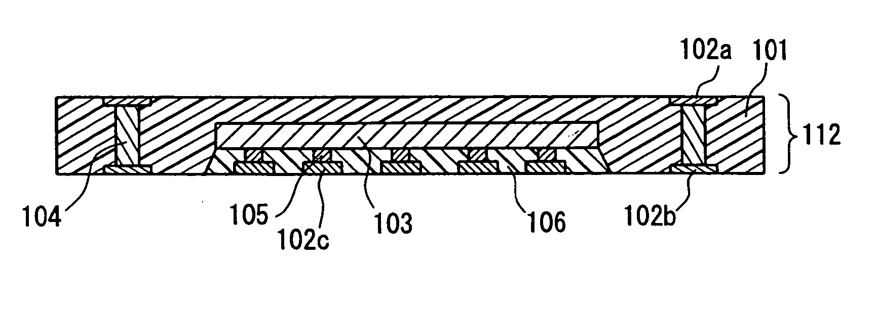
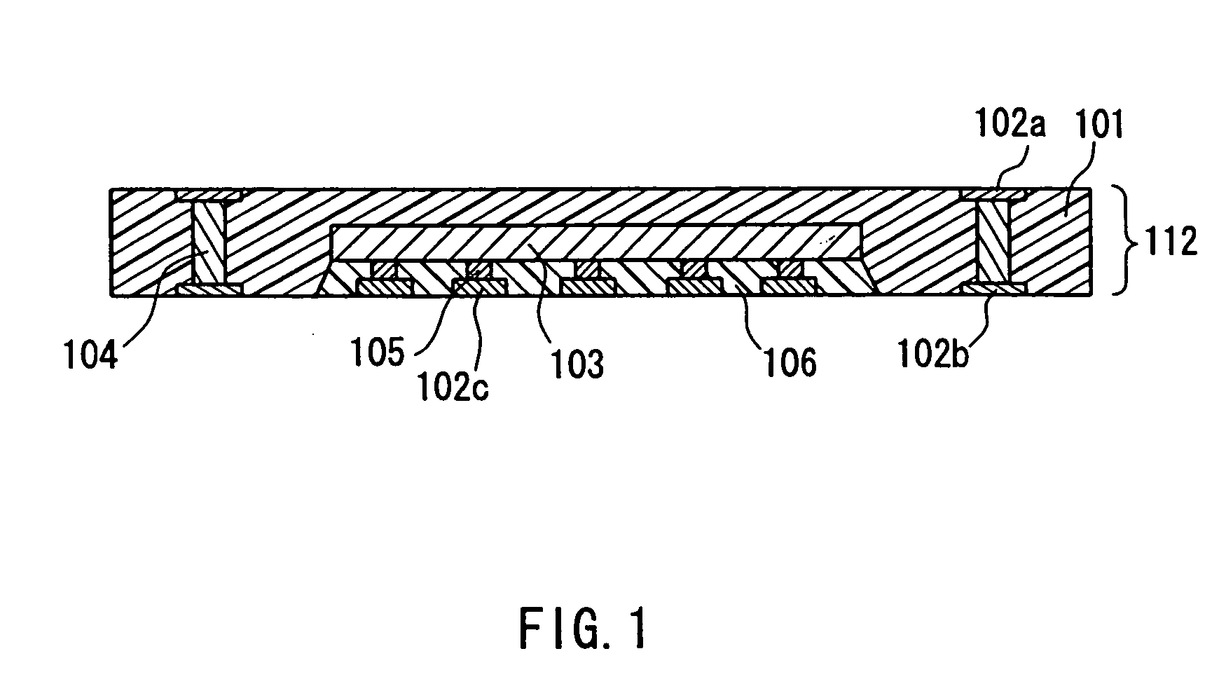
[0071] FIG. 3A illustrates a cross section of a circuit component built-in module 312 according to the present embodiment. The circuit component built-in module 312 is configured so that a semiconductor chip 303 in a wafer-level chip-scale package (wafer-level CSP) form having a sufficiently small chip thickness is incorporated in an electrical insulating substrate 301. A multilayer substrate 303a is integrated and incorporated additionally. 302a denotes a wiring pattern formed on a principal surface of the electrical insulating substrate 301, and 302b denotes a wiring pattern formed on the other principal surface of the electrical insulating substrate 301. Wiring patterns 302a and 302b are connected electrically with each other through inner vias 304 that pass through the electrical insulating substrate 301.

[0072] FIG. 3B illustrates an example of a configuration in which a wafer-level CSP 303a is mounted on a multilayer substrate 306 for rewiring. A circuit component built-in modu...

embodiment 3

[0081] FIG. 5 illustrates a cross section of a circuit component built-in module 512 according to the present embodiment. Members thereof corresponding to the circuit component built-in module 112 according to Embodiment 1 are made of the same materials processed in the same manners. The circuit component built-in module 512 is configured so that semiconductor chips 503a and 503b are incorporated in an electrical insulating substrate 501 in a state in which upper surfaces of the semiconductor chips 503a and 503b face each other. 502b and 502c denote wiring patterns formed on a principal surface of the electrical insulating substrate 301, and 502a and 502d denote wiring patterns formed on the other principal surface of the electrical insulating substrate 501. The wiring patterns 502a and 502b are connected electrically with each other through inner vias 504 that pass through the electrical insulating substrate 501. The semiconductor chips 503a and 503b are connected electrically with...

embodiment 4

[0090] FIG. 7B illustrates a cross section of a stacked module 712 according to the present embodiment. The stacked module 712 is configured so that circuit component built-in modules 112, each of which is according to Embodiment 1, are stacked.

[0091] The following describes an example of a method for manufacturing the stacked module 712 according to the present embodiment, while referring to FIGS. 7A and 7B.

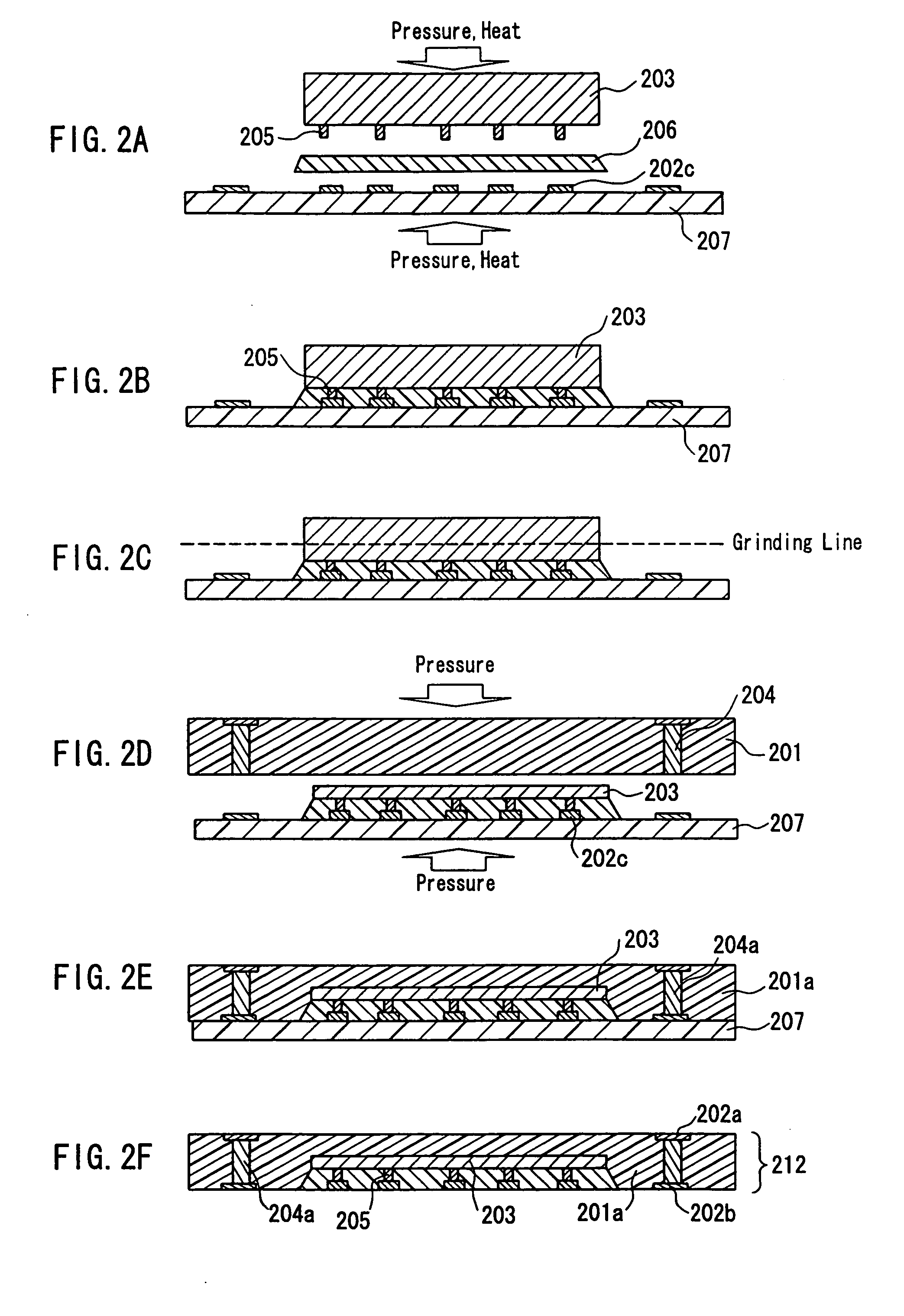
[0092] First of all, circuit component built-in modules 701a to 701d are produced (FIG. 7A) in the same manner as that in Embodiment 1 except for that the heating temperature is set to be in a range of 100.degree. C. to 130.degree. C. so that a mixture of a composite sheet 701 and a conductive resin composition in through holes 704 is maintained in a semi-cured or partially cured state (B-stage state).

[0093] Next, the circuit component built-in modules are stacked under a controlled pressure, so as to form a four-layer stacked module 712 (FIG. 7B). In FIGS. 7A and 7B, 702a and 7...


PUM


Abstract

A circuit component built-in module includes: a first electrical insulating substrate made of a mixture containing an inorganic filler and a thermosetting resin; a plurality of wiring patterns formed at least on a principal surface of the first electrical insulating substrate; a semiconductor chip incorporated in the first electrical insulating substrate and connected electrically with the wiring patterns; and inner vias electrically connecting the plurality of wiring patterns with one another, the inner vias passing through the first electrical insulating substrate. In the circuit component built-in module, the semiconductor chip has a thickness of not less than 30 mum and not more than 100 mum, and has a non-wired surface ground, and the circuit component built-in module has a thickness in a range of not less than 80 mum and not more than 200 mum. With this configuration, the high-performance and compact-size circuit component built-in module in which circuit components are mounted at a high density is provided so as to be used suitably in various types of electronic information devices.

Description

[0001] 1. Field of the Invention[0002] The present invention relates generally to a circuit component built-in module and a method for manufacturing the same. More specifically, it relates to a method for manufacturing a circuit component built-in module, in which semiconductor chips are incorporated in electrical insulating substrates for reducing the thickness and forming a stacked module, whereby the high-density mounting of components is achieved.[0003] 2. Related Background Art[0004] Following the tendency of electronic information devices toward high performance and compact size so as to be fit for the information communication industry that has developed remarkably in recent years, it is increasingly demanded to achieve high density, improved function, and shortened wiring of circuit components used in such electronic information devices. To achieve such characteristics, it is demanded increasingly to reduce the thickness of a module incorporating a circuit component or an el...

Claims


Application Information

Patent Timeline
IPC IPC(8): H01L21/56H01L21/60H01L21/98H01L23/498H01L23/538H01L25/065H01L25/10H05K1/18
CPCH01L21/56H01L21/563H01L23/49822H01L23/49833H01L23/5385H01L23/5389H01L24/81H01L25/0657H01L25/105H01L25/50H01L2224/13111H01L2224/13144H01L2224/73204H01L2224/81001H01L2224/81801H01L2224/83101H01L2224/83856H01L2225/06513H01L2225/06517H01L2225/06524H01L2225/06541H01L2225/06582H01L2225/06589H01L2225/06596H01L2924/01005H01L2924/01013H01L2924/01029H01L2924/0103H01L2924/01033H01L2924/01046H01L2924/01047H01L2924/0105H01L2924/01074H01L2924/01075H01L2924/01078H01L2924/01079H01L2924/01082H01L2924/14H01L2924/19041H01L2924/19042H01L2924/19043H01L2924/30105H01L2924/30107H05K1/187H01L2924/01006H01L2924/01019H01L2924/01024H01L2924/014H01L24/29H01L2924/0132H01L2924/0133H01L2224/16225H01L2224/32225H01L2924/1517H01L2225/1035H01L2225/1058H01L2225/107H01L2224/29111H01L2224/2919H01L2924/00H01L2924/01083H01L2924/3512H01L2924/00014H01L21/568H01L2224/32145H01L2924/15787H01L2224/45144H01L2924/1627H01L2224/04105H01L2224/73267
Inventor SUGAYA, YASUHIROASAHI, TOSHIYUKIKOMATSU, SHINGOYAMAMOTO, YOSHIYUKINAKATANI, SEIICHIYUHAKU, SATORUOHTANI, KAZUO
Owner PANASONIC CORP
Why Eureka
Try Eureka