
Apparatus, mold and method for producing substrate for plasma display panel

a technology of plasma display panel and substrate, which is applied in the manufacture of electrode systems, manufacturing tools, electric discharge tubes/lamps, etc., can solve the problems of unfavorable rib transfer, unfavorable rib transfer, and non-uniform dielectric layer molded, etc., to achieve the effect of reducing the defect of ribs and non-uniformity of the dielectric layer

Inactive Publication Date: 2004-08-26
3M INNOVATIVE PROPERTIES CO
View PDF24 Cites 16 Cited by
  • Summary
  • Abstract
  • Description
  • Claims
  • Application Information

AI Technical Summary

Benefits of technology

This approach ensures high accuracy and uniformity in producing ribs and dielectric layers, preventing defects and non-uniformity, while simplifying the process and reducing equipment requirements, enabling efficient production of high-quality substrates for PDPs across various sizes.

Problems solved by technology

Otherwise, there is a tendency that a non-uniform dielectric layer may be molded integrally with the ribs.
In case where the glass plate or mold have a comparatively wide area, this undesired tendency is increased.
According to this method, there is a fear that, when the mold is removed from the glass plate, peeling of the ribs from the glass plate can occur, thereby making it impossible to properly transfer the ribs to the glass plate.
It is usually required to use a pressure reducing device accompanying complicated constitution and complicated handling for such pressure reduction.
The pressure reducing device is large in size and often requires additional equipment.
Close contact under reduced pressure requires not only a wide space for such equipment, but also complicated step and skill.
However, according to both of these methods, there is a tendency that air bubbles are entrapped between the mold and plate upon close contact.
Such entrapment of air bubbles is likely to introduce defects into the ribs.
Particularly, in case where the substrate for PDP has a wide area, many defects can occur.
However, as described above, use of the pressure reducing device requires wide space and skill, which is not preferred.

Method used


Image

  • Apparatus, mold and method for producing substrate for plasma display panel
  • Apparatus, mold and method for producing substrate for plasma display panel
  • Apparatus, mold and method for producing substrate for plasma display panel

Examples


example 1

[0081] First, the following components were mixed in the weight ratio described below to prepare a mixed solution.

[0082] Aliphatic urethane acrylate oligomer (manufactured by Henkel Co. under the trade name of "Photomer 6010"):

[0083] 90 Parts by weight

[0084] Photocuring initiator (2-hydroxy-2-ethyl-1-phenyl-propan-1-one, manufactured by Clariant Co. under the trade name of "Darocure 1173"):

[0085] 1 Part by weight

[0086] High dielectric medium (propylene carbonate, manufactured by Wako Pure Chemical Industries Co., Ltd.):

[0087] 8.1 Parts by weight

[0088] Ionic conductive substance (lithium perchlorate, manufactured by Wako Pure Chemical Industries Co., Ltd.):

[0089] 0.9 Parts by weight

[0090] A polyethylene terephthalate (PET) film having a thickness of 50 .mu.m was finely cut to make two film pieces (30 cm in width and 20 cm in length).

[0091] Next, 5 cm.sup.3 of the above mixed solution was dropped on one of two film pieces thus obtained. Then, one film piece was laid via the mixed solu...

example 2

[0112] The same procedure as in Example 1 was repeated, except that the following components (which are the same as those used in Example I) were mixed in the weight ratio described below to prepare a mixed solution in this example, and a sheet was made. Aliphatic urethane acrylate oligomer:96 Parts by weight

[0113] Photocuring initiator:

[0114] 1 Part by weight

[0115] High dielectric medium:

[0116] 3.6 Parts by weight

[0117] Ionic conductive substance:

[0118] 0.4 Parts by weight

[0119] In the same manner as in Example 1, the surface resistance and electrostatic voltage of the resulting sheet were measured. As a result, the following measurement results were obtained.

[0120] Surface resistance of sheet: 3.3.times.10.sup.10 .OMEGA. / .quadrature..

[0121] Electrostatic voltage of sheet: nearly 0 V

[0122] The surface resistance of the sheet of this example is higher that that of Example 1. However, the electrostatic voltage is nearly 0 V and the sheet is hardly charged actually. Accordingly, it is...

example 3

[0124] The same procedure as in Example 1 was repeated, except that the following components (which are the same as those used in Example 1) were mixed in the weight ratio described below to prepare a mixed solution in this example, and a sheet was made.

[0125] Aliphatic urethane acrylate oligomer:

[0126] 99 Parts by weight

[0127] Photocuring initiator:

[0128] 1 Part by weight

[0129] In the same manner as in Example 1, the surface resistance and electrostatic voltage of the resulting sheet were measured. As a result, the following measurement results were obtained.

[0130] Surface resistance of sheet: 2.0.times.10.sup.14 .OMEGA. / .quadrature. or more

[0131] Electrostatic voltage of sheet: 2000 V or higher

[0132] The surface resistance of the sheet of this example is higher that that of Example 1. Furthermore, the electrostatic voltage is 2000 V or higher and the sheet is actually charged. Accordingly, it is found that the surface resistance of this example is not a low value enough to prevent...


PUM

PropertyMeasurementUnit
diameteraaaaaaaaaa
diameteraaaaaaaaaa
viscosityaaaaaaaaaa

Abstract

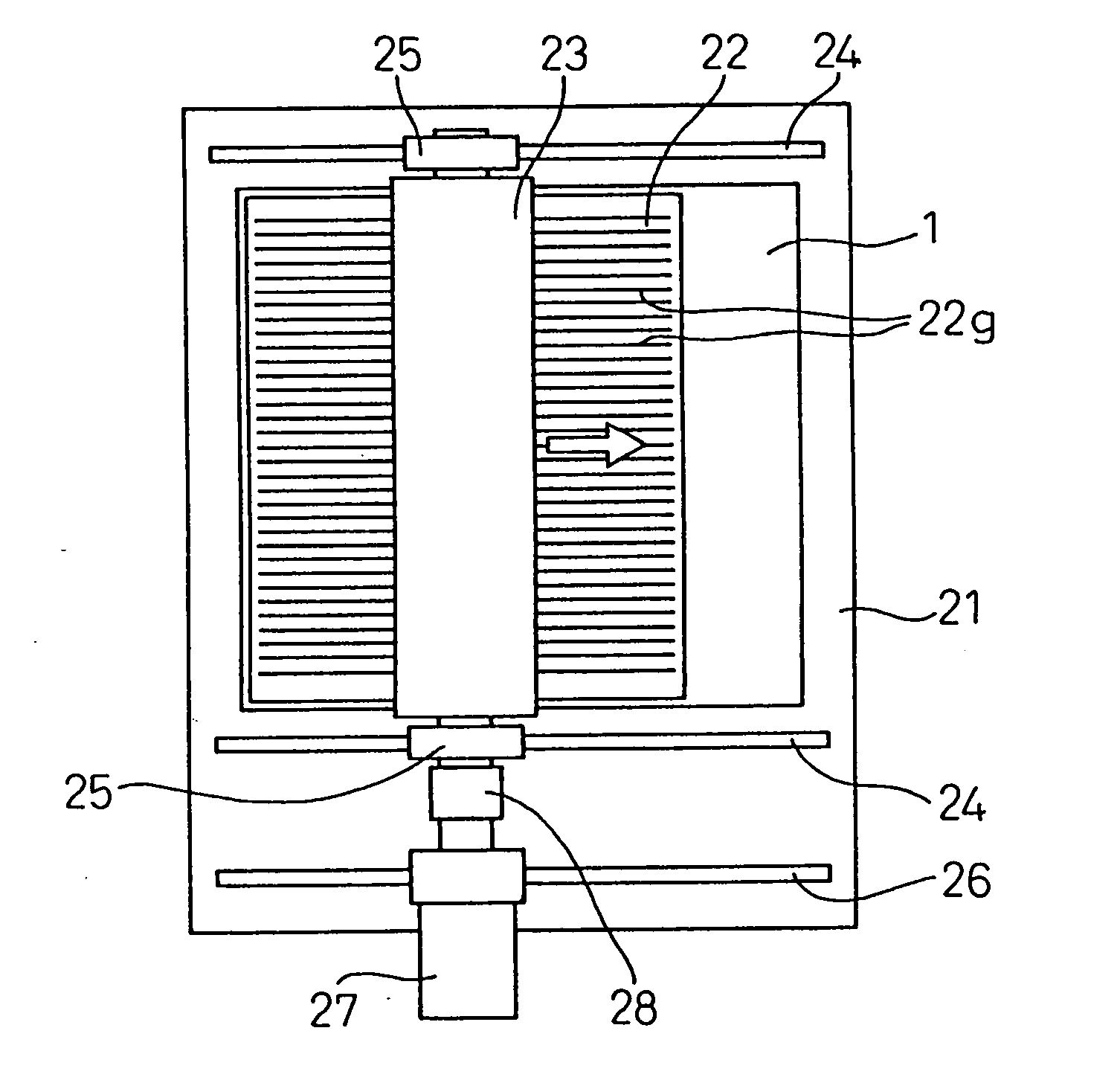
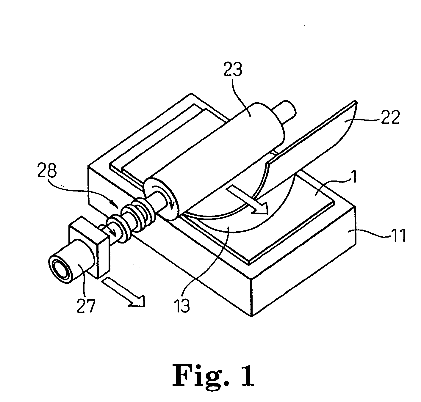
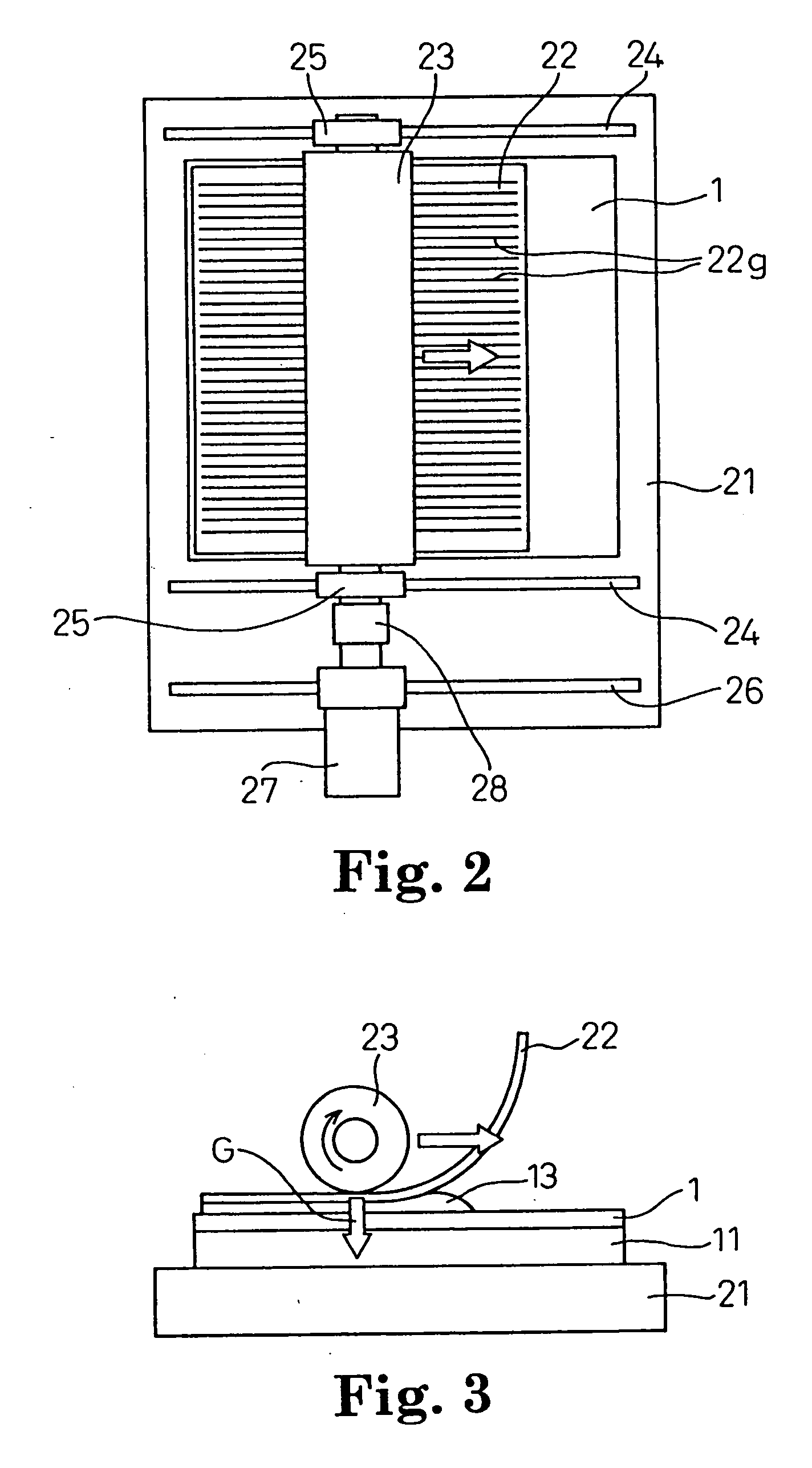
An apparatus is provided for producing a substrate for PDP, which can easily reduce ununiformity of a dielectric layer and defects of ribs. The apparatus is so constituted that it comprises: a table for the plate, a rib precursor supplying portion for providing a precursor of the ribs on the plate, a pliable mold having at least groove portions provided in parallel with each other at a fixed distance, which is disposed on the precursor of the ribs provided on the plate, a mold pressing portion for applying a pressure to the mold, thereby to contact the mold closely with the plate via the precursor of the ribs, and a driving portion for moving the mold pressing portion along the groove portions of the mold.

Description

[0001] The present invention belongs to the field of plasma display panels (hereinafter also referred to as "PDP") and, more particularly, it relates to an apparatus for producing a substrate for PDP, a mold used in such production apparatus, and a method of producing a substrate for PDP.[0002] Recently, thin display devices such as PDPs have been developed intensively. Because PDPs are thin and can also provide a large image plane, high image quality and wide viewing angle can be achieved as compared with a typical thin display device such as liquid crystal display.[0003] Generally, PDP is equipped with a substrate. Typical substrates for PDP is composed of a pair of glass flat plates facing each other at a distance via ribs each having the same dimension (also referred to as a barrier rib, bulkhead or barrier). Such ribs of the substrate for PDP with such a constitution can partition the space between a pair of glass plates in an air-tight manner to form a plurality of discharge d...

Claims


Application Information

Patent Timeline
Patent Type & Authority Applications(United States)
IPC IPC(8): H01J9/24
CPCH01J9/241H01J2211/36H01J9/242
Inventor KIKUCHI, HIROSHIYOKOYAMA, CHIKAFUMIYODA, AKIRASUGIMOTO, TAKAKISUWA, TOSHIHIRO
Owner 3M INNOVATIVE PROPERTIES CO
Learn More