Atomic layer deposition for high temperature superconductor material synthesis
- Summary
- Abstract
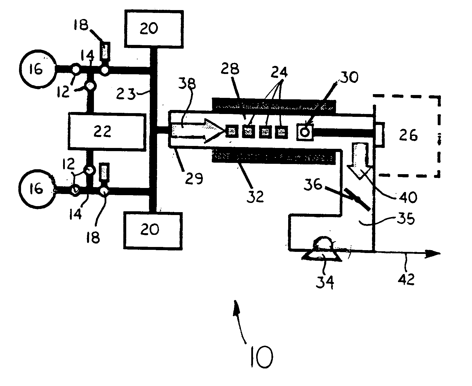
- Description
- Claims
- Application Information
AI Technical Summary
Benefits of technology
Problems solved by technology
Method used
Image

Examples
Embodiment Construction
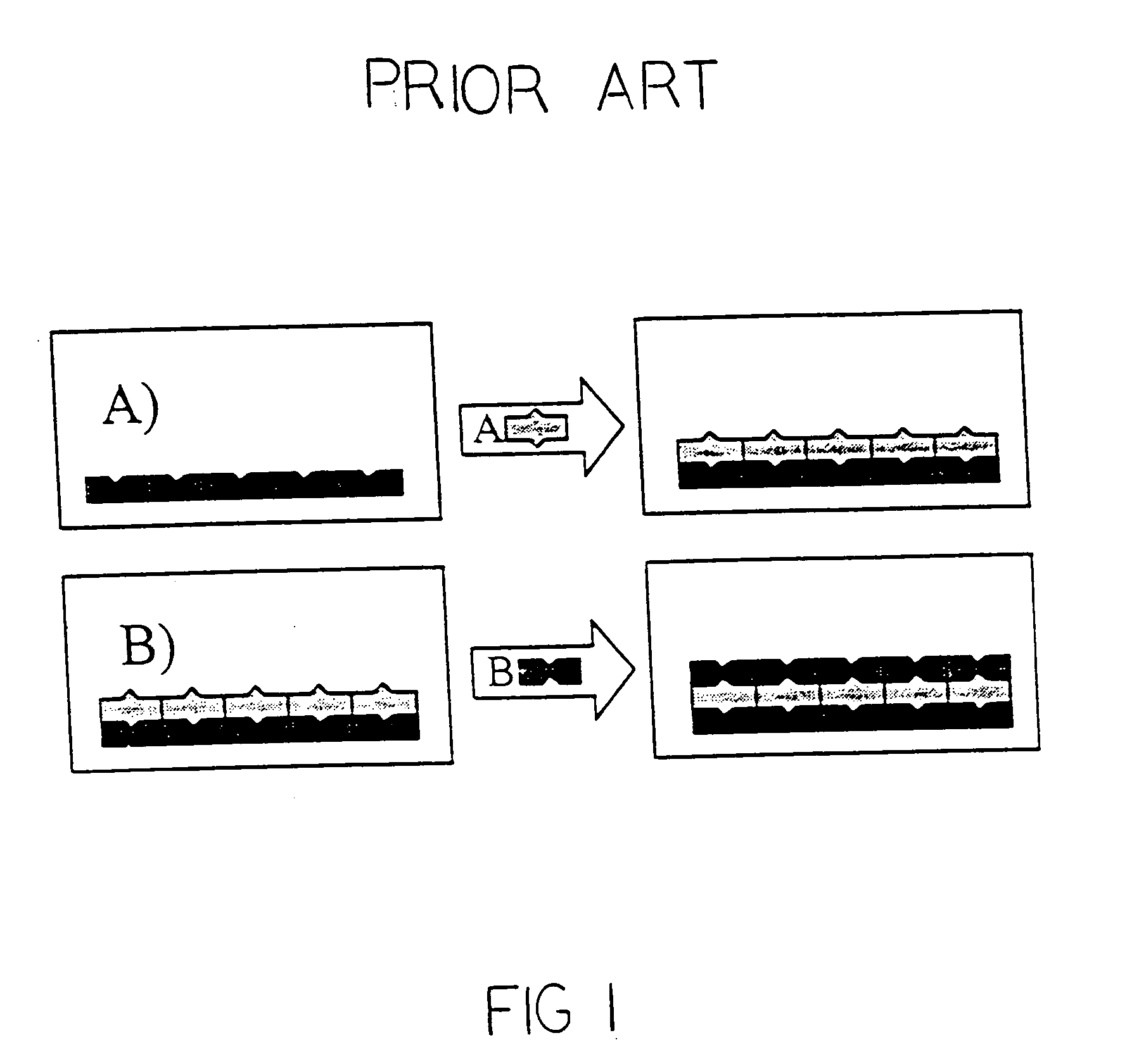
[0075] Consider the following binary A-B reaction cycle, illustrated by Equations 1 and 2, for the ALD of alumina, Al.sub.2O.sub.3 via the reaction of trimethyl aluminum (TMA) with hydroxyl (OH).
Reaction .vertline.--Al--Al--OH*+Al(CH.sub.3).sub.3.fwdarw..vertline.--Al---O--Al(CH.sub.3).sub.2*+CH.sub.4 Equation 1
Reaction B .vertline.--Al--O--Al(CH.sub.3).sub.2*+2H.sub.2O.fwdarw..vertli-ne.--Al--O--Al--OH*+2CH.sub.4 Equation 2
[0076] In Equations 1 and 2, the asterisks designate moieties adsorbed to the substrate surface, the ".vertline.--" indicates the substrate surface, and the equations have been simplified to show only one surface active site. The actual scheme involves several active sites at once. In Equation 1, the substrate surface is initially covered with hydroxyl (OH) moieties formed by exposure of the Alumina substrate's surface to water. The hydroxyl moieties react with TMA to deposit a monolayer of aluminum atoms that are terminated by methyl (CH.sub.3) species, and rele...
PUM
| Property | Measurement | Unit |
|---|---|---|
| Time | aaaaa | aaaaa |
| Angle | aaaaa | aaaaa |
| Length | aaaaa | aaaaa |
Abstract
Description
Claims
Application Information
 - Generate Ideas
- Intellectual Property
- Life Sciences
- Materials
- Tech Scout
- Unparalleled Data Quality
- Higher Quality Content
- 60% Fewer Hallucinations
Browse by: Latest US Patents, China's latest patents, Technical Efficacy Thesaurus, Application Domain, Technology Topic, Popular Technical Reports.
© 2025 PatSnap. All rights reserved.Legal|Privacy policy|Modern Slavery Act Transparency Statement|Sitemap|About US| Contact US: help@patsnap.com