Display panel, electronic apparatus with the same, and method of manufacturing the same

a technology of electronic equipment and display panels, applied in the field of display panels, can solve the problems of reducing the contrast of the display device, reducing the quality of the display image, and existing organic el elements not simultaneously realizing high luminance and a long lifespan, and achieves the effects of high integration of elements, high function, and effective manufacturing of the panel

Active Publication Date: 2004-09-16
SEIKO EPSON CORP
View PDF17 Cites 31 Cited by
  • Summary
  • Abstract
  • Description
  • Claims
  • Application Information

AI Technical Summary

Benefits of technology

0036] According to the present invention, the formation of other circuits including the control elements and the deposition of the first or second low reflection layer may be performed with the same material by a series of process or a mixed process, and the equipment may be shared. As such, it is possible to effectively manufacture the panel and to cope with the miniaturization and high integration of element. Further, even if a display panel with a high function and high precision is manufactured, an increase in cost can be suppressed.
0037] In addition, the display panel according to the present invention comprises a black layer having a function of reducing a step difference at a lower portion and light-emitting elements prov...

Problems solved by technology

As such, the contrast of the display device is reduced, thereby reducing the quality of the display image.
However, existing organic EL elements do not simultaneously realize high luminance and a long lifespan.
As such, it is impossible to avoid a reduction in visibility due to the effect of light incident from the exterior out of doors.
In these conventional display devices, since an expensive member, such as a circular polarizing p...

Method used


Image

  • Display panel, electronic apparatus with the same, and method of manufacturing the same
  • Display panel, electronic apparatus with the same, and method of manufacturing the same
  • Display panel, electronic apparatus with the same, and method of manufacturing the same

Examples


first embodiment

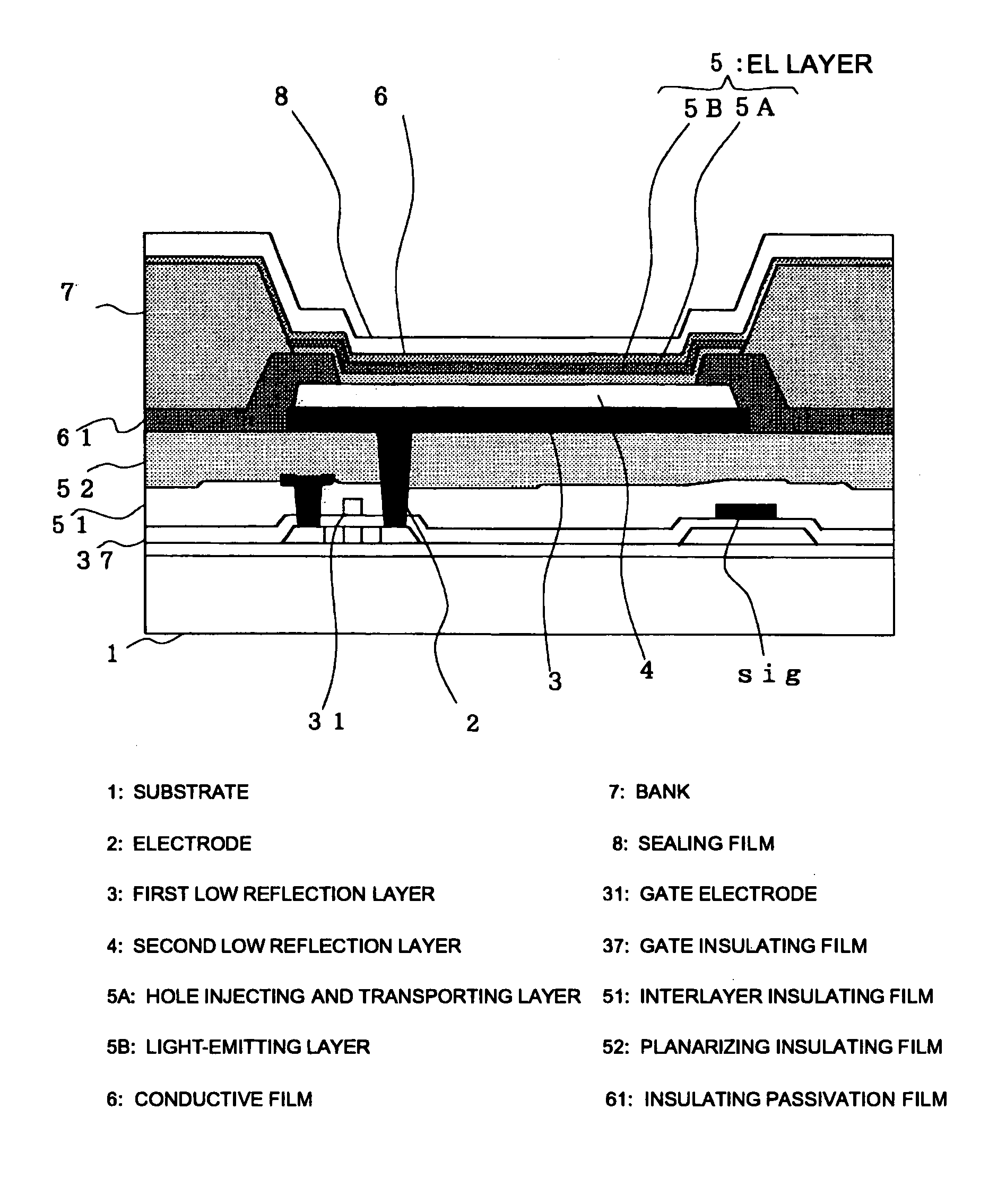
[0108] FIG. 1 is a cross-sectional view showing a part of the display panel according to a first embodiment of the present invention. In FIG. 1, reference numeral 1 indicates a substrate. In this embodiment, the substrate 1 is provided with thin film transistors (hereinafter, referred to as TFTs) serving as control elements (driving elements) (only a second TFT 30 to be described later is shown in FIG. 1).

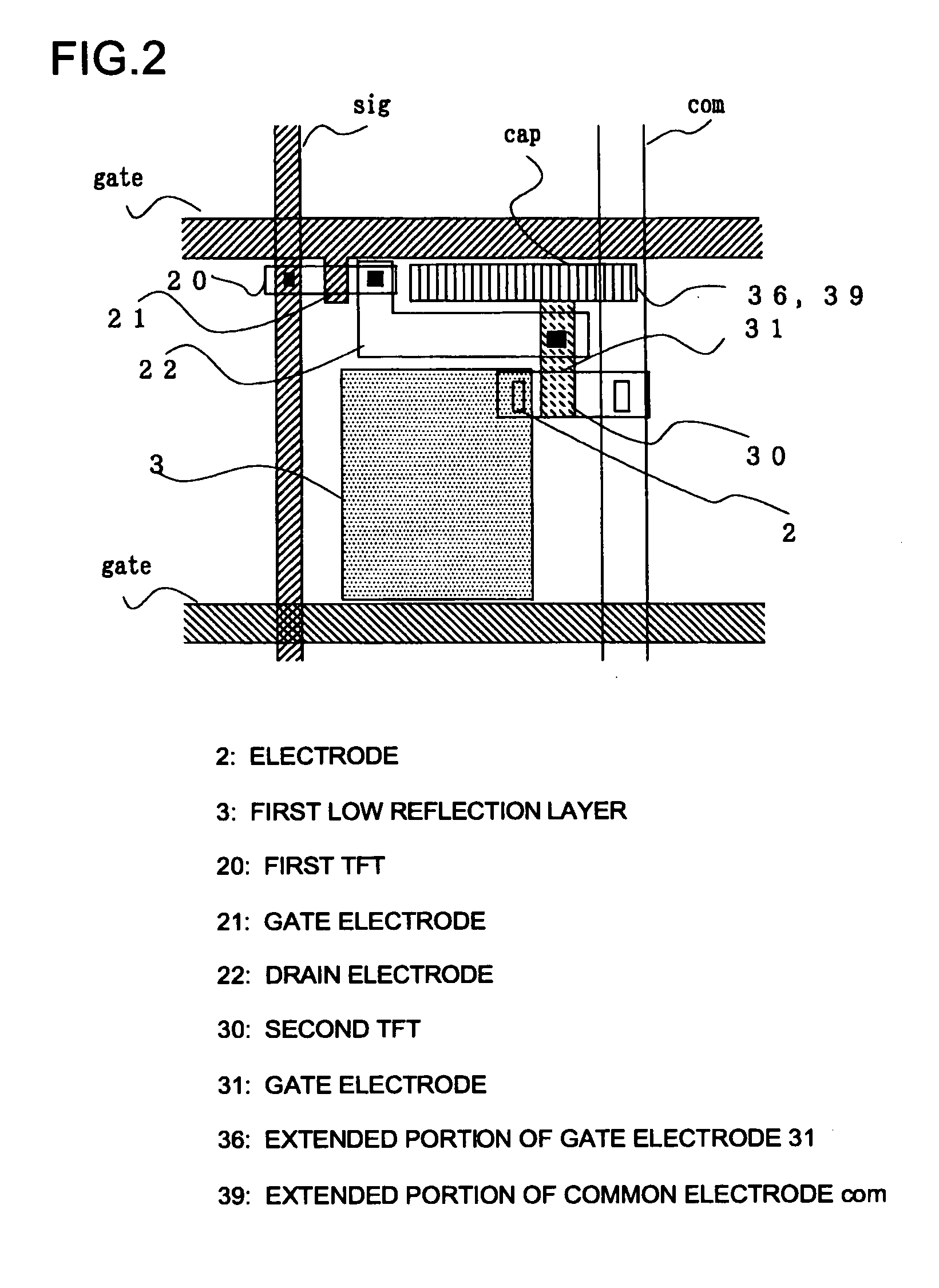
[0109] FIG. 2 is a plane view showing one pixel constituting a display panel. FIG. 2 shows elements formed mostly between a second low reflection layer 4 (first low reflection layer 3) and the substrate. A gate electrode of a first TFT 20 is supplied with scanning signals via a scanning line `gate`. A storage capacitor `cap` is adapted to hold image signals supplied from a data line `sig` via the first TFT 20. A gate electrode 31 of a second TFT 30 is supplied with the image signal held by the storage capacitor `cap`.

[0110] The first TFT 20 and the second TFT 30 are formed of an is...

second embodiment

[0133] FIG. 8 is a cross-sectional view showing a part of the display panel according to a second embodiment of the present invention. Elements indicated by the same reference numerals as those in FIG. 1 correspond to those described in the first embodiment, and thus the description thereof will be omitted herein. Although FIG. 8 shows only a part that is required for the description of this embodiment, the structure of this embodiment is not different from that of the first embodiment. Reference numeral 11 indicates a black layer (combining the aforementioned planarizing insulating film 52) into which an insulating photosensitive resin containing a black pigment is solidified. Further, reference numeral 5A indicates a hole injecting and transporting layer, and reference numeral 5B indicates a light-emitting layer, which are parts of the EL layer 5. In addition, ITO used for the second low reflection layer 4 may be used for the hole injecting and transporting layer 5A.

[0134] In this...

third embodiment

[0139] FIG. 11 is a cross-sectional view showing a part of the display panel according to a third embodiment of the present invention. Elements indicated by the same reference numerals as those in FIG. 8 are the same or equivalent as those described in the first and second embodiments, and thus the description thereof will be omitted herein. Reference numeral 11A indicates a black layer formed of an allotrope of carbon having conductivity.

[0140] In the present embodiment, the black layer 11A absorbs the light incident from the exterior to decrease the reflecting light and thus reduces reflectance, as similar to the second embodiment. In this embodiment, the black layer 11A is formed of an allotrope of carbon. Since the black layer 11A is made of carbon having conductivity, it is not necessary to electrically connect the electrode 2 to the hole injecting and transporting layer 5A directly.

[0141] Next, a method of manufacturing the display panel according to the present embodiment wil...


PUM


Abstract

There is provided a display panel that is capable of improving visibility outdoors and which can be easily manufactured. In a display panel in which at least one side thereof serves as a display surface, the display panel includes a first reflectance layer 3, which is made of titanium, titanium nitride, or an alloy of titanium and tungsten and a second reflectance layer 4, which is made of indium tin oxide, indium zinc oxide, or gallium zinc oxide, wherein the first and second low reflection layer 3 and 4 are deposited at positions corresponding to pixels on a substrate 1.

Description

[0001] The present invention relates to a display panel and the like. More particularly, the present invention is directed to improve low visibility due to the reflection of light incident from the exterior.[0002] Recently, display devices utilizing a liquid crystal display (LCD), an organic electroluminescent element (hereinafter, referred to as `an organic EL element`), and the like are employed in various electronics, such as a cellular phone, a personal computer, an electronic organizer, a portable electronic game console, and the like. As such, users have many opportunities to look at a display screen of the electronic apparatus outdoors as well as looking at the screen indoors.[0003] This case discusses in which light is incident on the display screen from the exterior. The incident light is reflected from the screen back to viewers. However, more intense light is incident on the screen and is reflected from the screen back to the viewers not indoors, but outdoors. As such, th...

Claims


Application Information

Patent Timeline
IPC IPC(8): G09F9/00G09F9/30H05B33/10H01L27/32H01L51/50H01L51/52H05B33/00H05B33/14H05B33/22H05B33/24H05B33/26
CPCH01L27/3244H01L51/5237H01L2251/5315H01L51/5284H01L51/529H01L51/5281H10K59/12H10K50/81H10K50/818H10K50/8426H10K50/86H10K50/87H10K50/865H10K2102/3026
Inventor KARASAWA, YASUSHINOJIMA, SHIGEONOZAWA, RYOICHI
Owner SEIKO EPSON CORP
Why Eureka
Try Eureka