Display device and electronic apparatus

a technology of electronic equipment and display device, which is applied in the direction of mould pallets, identification means, instruments, etc., can solve the problems of complex product and process management procedures affecting the distribution process, requiring a great amount of effort, and unable to let each product have product identification information

Active Publication Date: 2004-09-30
BOE TECH GRP CO LTD
View PDF29 Cites 92 Cited by
  • Summary
  • Abstract
  • Description
  • Claims
  • Application Information

AI Technical Summary

Problems solved by technology

In particular, after dividing the mother boards into individual cells, it is difficult to let each product have product identification information, such as a lot number, a mother board number, and a product number and product record information, such as a manufacturing factory and the date of manufacture.
Such complicated product and process management procedures affect distribution processes as well as production processes.
In such an environment, there may be no space to attach an IC tag to a liquid crystal display device or, even if there is a space for attaching an IC tag to a liquid crystal display device, it requires a great amount of effort and takes a long time to attach a ...

Method used


Image

  • Display device and electronic apparatus
  • Display device and electronic apparatus
  • Display device and electronic apparatus

Examples


first exemplary embodiment

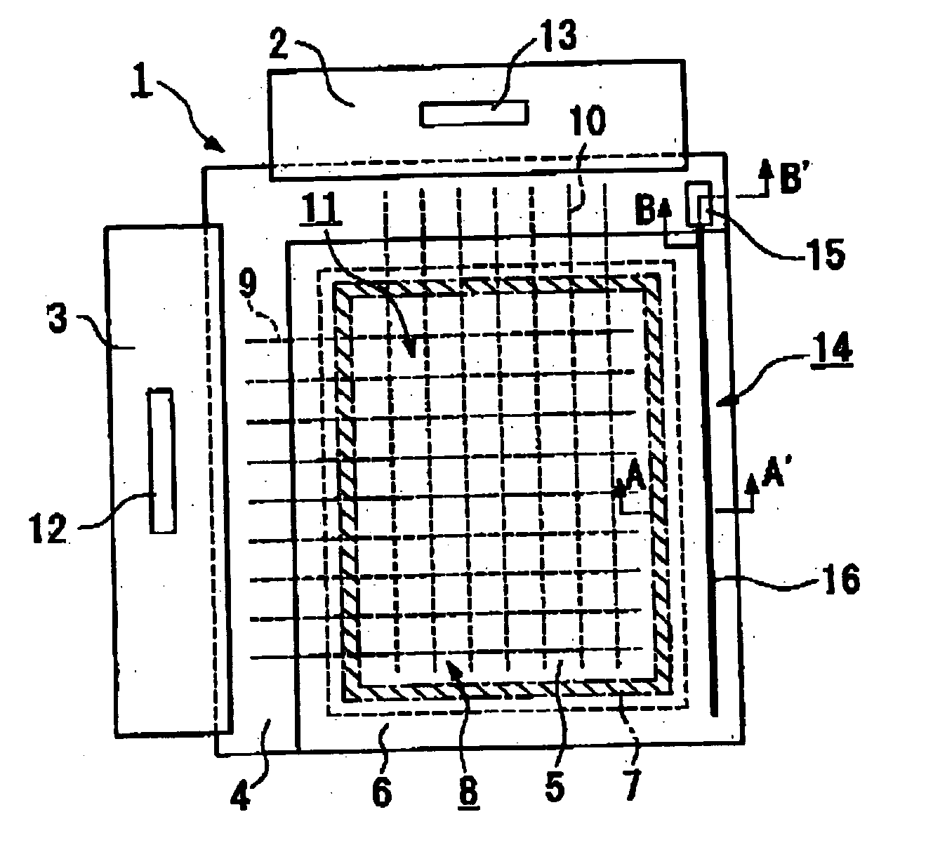
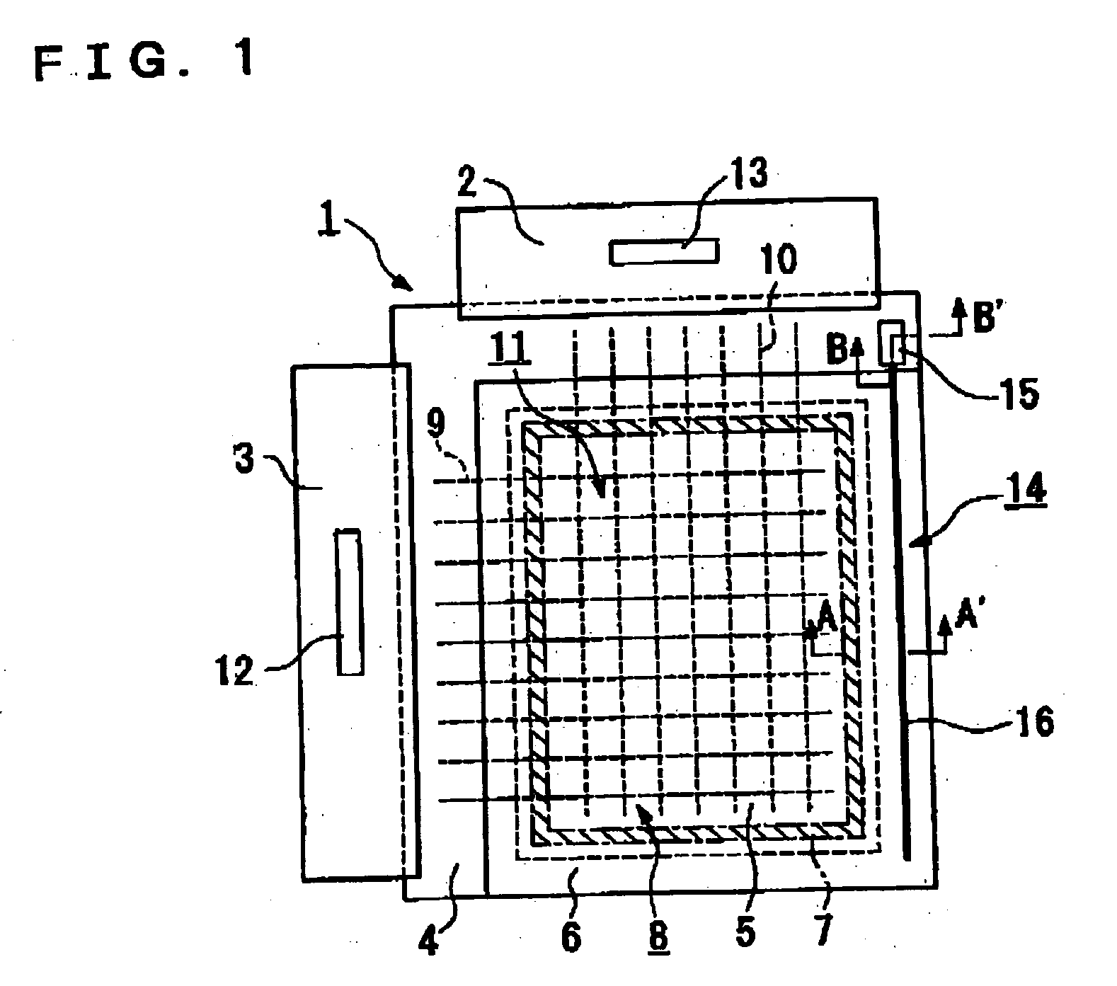
[0094] A first exemplary embodiment of the present invention will be described with reference to FIGS. 1 to 7.

[0095] A display device according to the present exemplary embodiment is an example of a transmissive liquid crystal display device in an active matrix using an amorphous silicon thin film transistor (TFT) as a pixel switching element.

[0096] In the respective drawings, in order to make the respective components visualized, the reduced scales of the respective components vary.

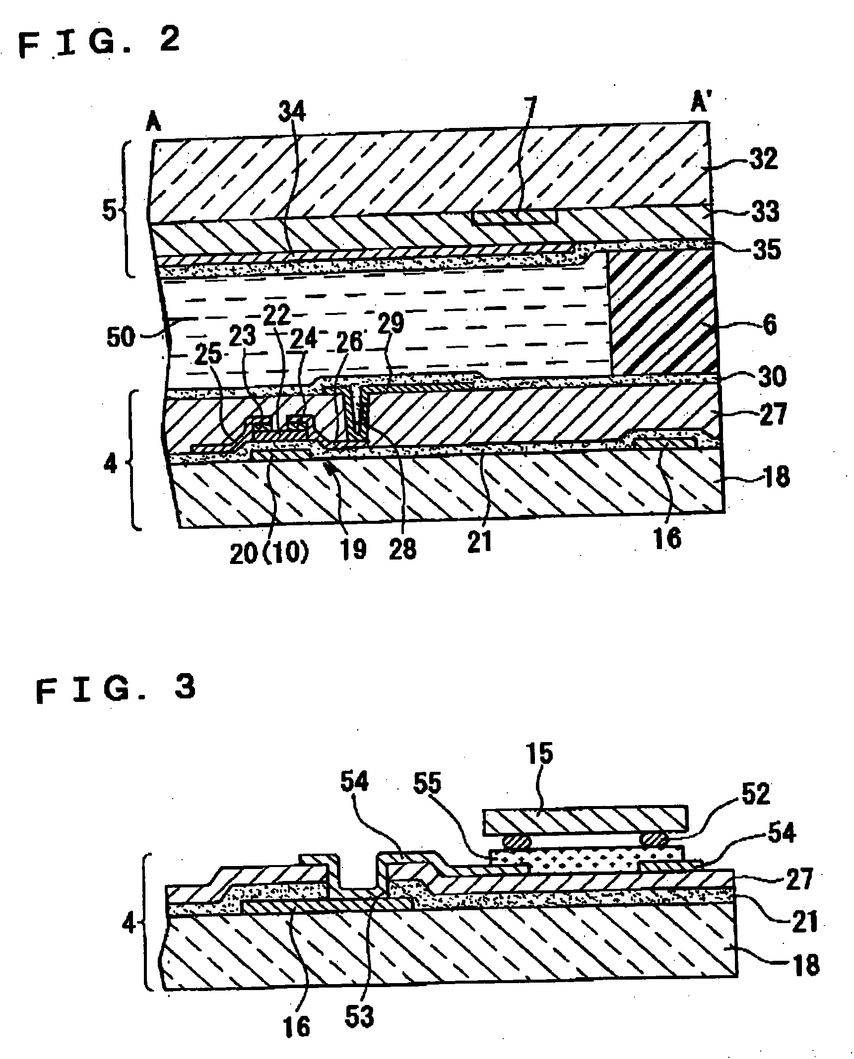
[0097] The liquid crystal display device according to the present exemplary embodiment includes a liquid crystal cell 1 and two FPCs 2 and 3 (external substrates) connected to the liquid crystal cell 1, as illustrated in FIGS. 1 and 2. The liquid crystal cell 1 includes a rectangular element substrate 4 and a counter substrate 5. A liquid crystal layer 50 is interposed between the element substrate 4 and the counter substrate 5. The width and the length of the element substrate 4 are larger than the widt...

second exemplary embodiment

[0109] A second exemplary embodiment of the present invention will now be described with reference to FIGS. 8 and 9.

[0110] The basic structure of the liquid crystal display device according to the present exemplary embodiment is the same as the structure of the first exemplary embodiment excluding the position in which the IC chip is mounted and the structure of the antenna in accordance with the position of the IC chip.

[0111] In FIGS. 8 and 9, the same components as those of FIGS. 1 to 3 are denoted by the same reference numerals and the detailed description thereof will be omitted.

[0112] According to the first exemplary embodiment, the IC chip 15 is mounted on the element substrate 4 of the liquid crystal cell 1. The entire antenna 16 is formed on the element substrate 4. On the other hand, according to the present exemplary embodiment, as illustrated in FIG. 8, the IC chip 15 is mounted on the FPC 2 (an external substrate). The antenna 16 is constituted of the first antenna 16a f...

third exemplary embodiment

[0117] A third exemplary embodiment of the present invention will be described with reference to FIG. 10.

[0118] A display device according to the first and second exemplary embodiments is a liquid crystal display device using an amorphous silicon TFT as a pixel switching element. On the other hand, a display device according to the present exemplary embodiment is a liquid crystal display device using polycrystalline silicon TFT or a single crystal silicon TFT as a pixel switching element.

[0119] The amorphous silicon TFT cannot constitute a communication integrated circuit in an IC chip that constitutes a radio communication device in consideration of driving ability as a transistor. The polycrystalline silicon TFTs or the single crystal silicon TFTs have enough driving ability to thus constitute the communication integrated circuit. Therefore, according to the present exemplary embodiment, as illustrated in FIG. 10, a communication integrated circuit 71 (a communication integrated-c...


PUM

PropertyMeasurementUnit
Poweraaaaaaaaaa

Abstract

To provide a display device and an electronic apparatus including a radio communication device, such as an IC tag, which do not need a special space to attach the IC tag and is capable of reducing the amount of time and effort required for attaching the IC tag, a display device including a radio communication device having at least one substrate provided with a display unit and display-unit-driving wiring lines 9 and 10, a communication integrated-circuit unit, and an antenna is provided. At least a part of the antenna is formed on the substrate and formed of a conductor formed in the same layer as a conductor that constitute the display unit or conductors that constitute the display-unit-driving wiring lines.

Description

[0001] 1. Field of Invention[0002] The present invention relates to a display device including a radio communication device and an electronic apparatus.[0003] 2. Description of Related Art[0004] A production method to obtain a plurality of liquid crystal cell patterns, in which the plurality of liquid crystal cell patterns are simultaneously formed on one mother board, two mother boards are attached to each other, and the mother boards are divided into individual cells, has been adopted for a display device, such as a liquid crystal display. Japanese Unexamined Patent Application Publication No. 2002-268042. The production method is extremely effective. However, according to the production method, after dividing the mother boards into individual cells, many additional processes, such as connection of a driving flexible printed circuit (hereinafter "FPC") must be performed before a complete liquid crystal module product is provided. In particular, after dividing the mother boards int...

Claims


Application Information

Patent Timeline
IPC IPC(8): B42D15/10G02F1/1345G06K19/00G06K19/07G06K19/077G09F9/30G09G3/20G09G3/36G09G5/00
CPCG06K19/07749G09G3/20G09G3/3648H01L2924/01019H01L2224/16H01L2924/3025G09G2380/04H01L2924/00014H01L2224/0401B28B1/0873B28B3/021B28B7/0055B28B7/007B28B7/0097B28B7/162B28B7/241E02D29/02
Inventor SATO, TAKASHI
Owner BOE TECH GRP CO LTD
Why Eureka
Try Eureka