Optical recording medium, method for manufacturing the same and target used for sputtering process
- Summary
- Abstract
- Description
- Claims
- Application Information
AI Technical Summary
Benefits of technology
Problems solved by technology
Method used
Image
Examples
working example 1
[0135] An optical recording medium sample #1-1 was fabricated in the following manner.
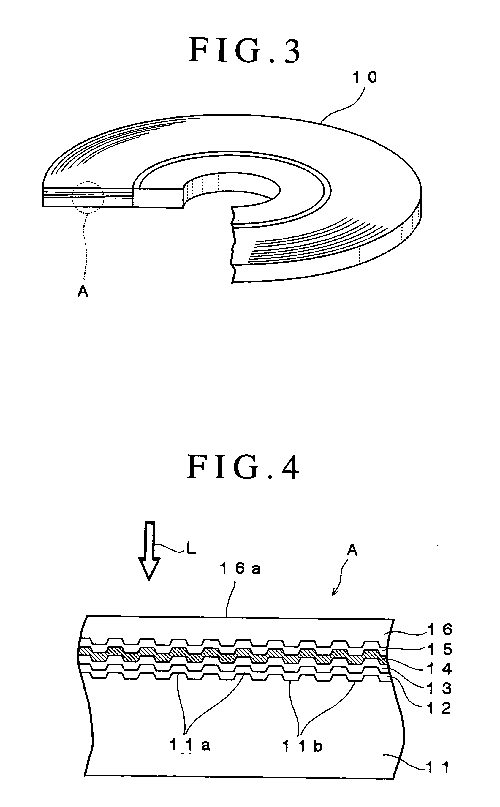
[0136] A disk-like polycarbonate substrate having a thickness of 1.1 mm and a diameter of 120 mm and formed with grooves and lands on the surface thereof was first fabricated by an injection molding process so that the track pitch (groove pitch) was equal to 0.32 .mu.m.
[0137] Then, the polyearbonate substrate was set on a sputtering apparatus and a reflective layer consisting of an alloy containing Ag, Pd and Cu and having a thickness of 100 nm, a second dielectric layer containing a mixture of ZnS and SiO.sub.2 and having a thickness of 35 nm, a recording layer containing as a primary component an alloy containing Fe and Al and having a thickness of 10 nm and a first dielectric film containing the mixture of ZnS and SiO.sub.2 and having a thickness of 20 nm were sequentially formed on the surface of the polycarbonate substrate on which the grooves and lands were formed, using the sputtering proces...
PUM
| Property | Measurement | Unit |
|---|---|---|
| Dielectric polarization enthalpy | aaaaa | aaaaa |
Abstract
Description
Claims
Application Information


