Method for making a nano-stamp and for forming, with the stamp, nano-size elements on a substrate

a nano-stamp and stamping technology, applied in the field of nano-stamping stamping, can solve the problems of limited lithograph process resolution by half a wavelength of electromagnetic radiation, no pattern is currently able to mass-produce elements below 50 nm, and no technology is currently able to achieve the effect of reducing the number of stamps

Inactive Publication Date: 2004-10-07
PECHENIK ALEXANDER
View PDF26 Cites 25 Cited by
  • Summary
  • Abstract
  • Description
  • Claims
  • Application Information

AI Technical Summary

Problems solved by technology

Optical lithography has been the key for the industrial production of these devices; however, it is well known in the art of lithography that the resolution of the lithographs process is limited by half a wavelength of the electromagnetic radiation.
All of these technologies suffer from serious drawbacks and none is currently able to mass-produce patterns having elements below 50 nm.
62, 2989 (1993) reported this kind of resolution, however their approach cannot be practically adapted for industrial production of nano-size patterns.
However, X-ray lithography has not yet shown its ability to go below 50 nm in an industrial fashion.
Atomic scanning probes have shown lithographic resolution below 10 nm, but this procedure is inherently slow and it is yet to be determined if the ASP can fabricate the nano-patterns with necessary speed for mass p

Method used


Image

  • Method for making a nano-stamp and for forming, with the stamp, nano-size elements on a substrate
  • Method for making a nano-stamp and for forming, with the stamp, nano-size elements on a substrate
  • Method for making a nano-stamp and for forming, with the stamp, nano-size elements on a substrate

Examples


Embodiment Construction

)

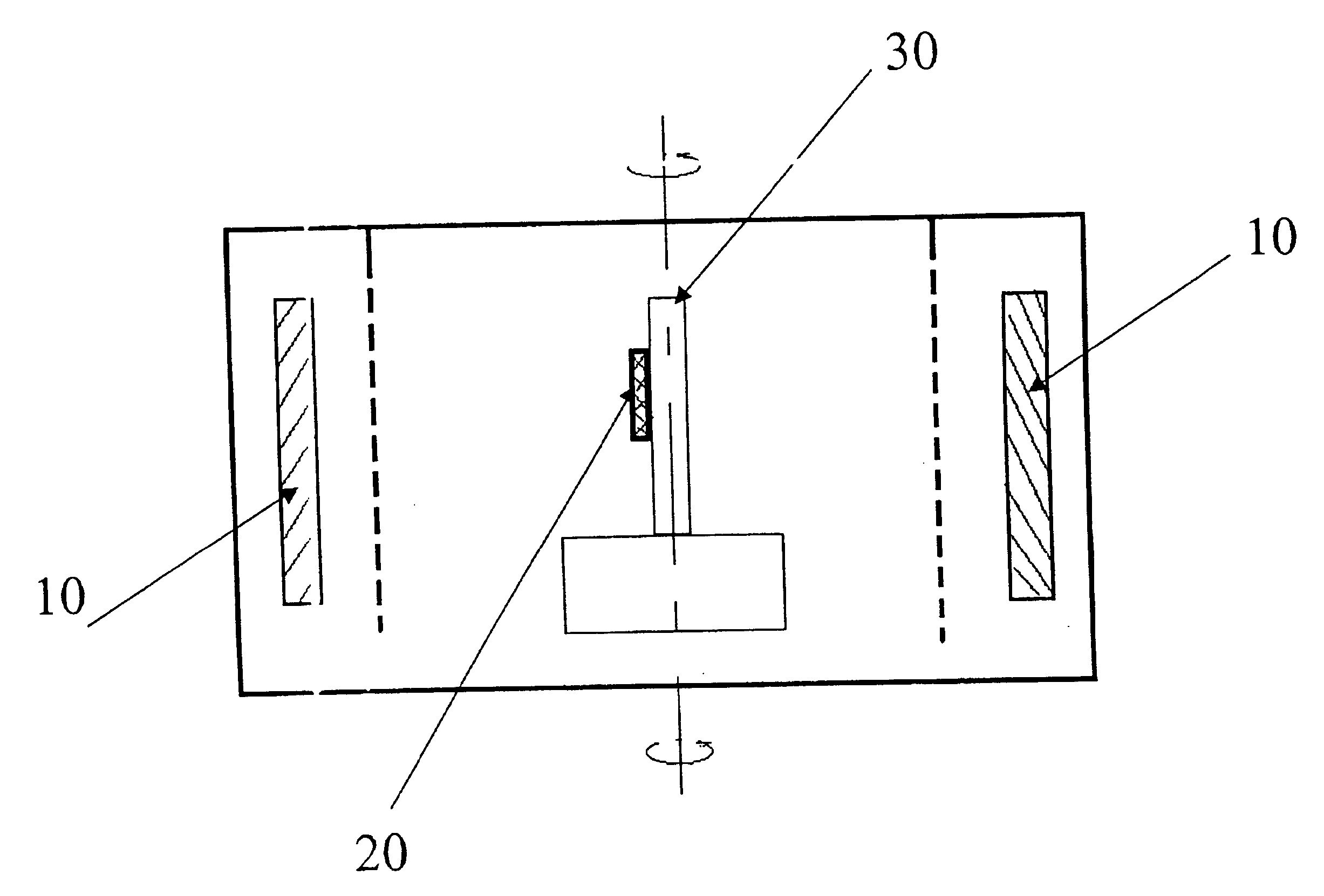
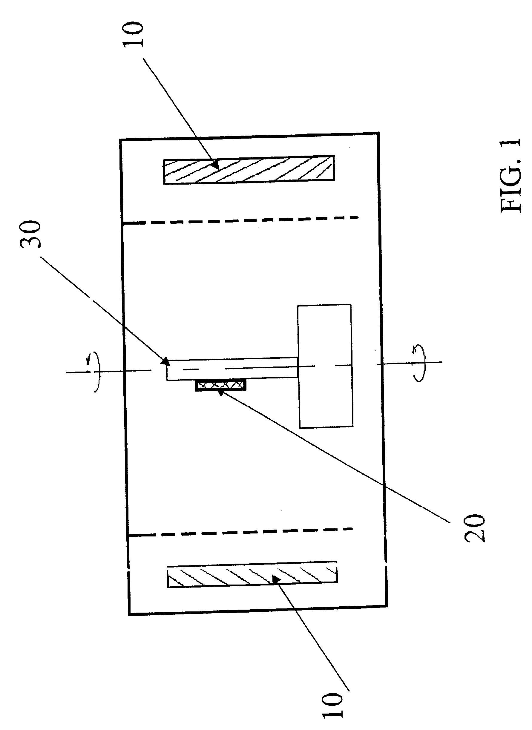
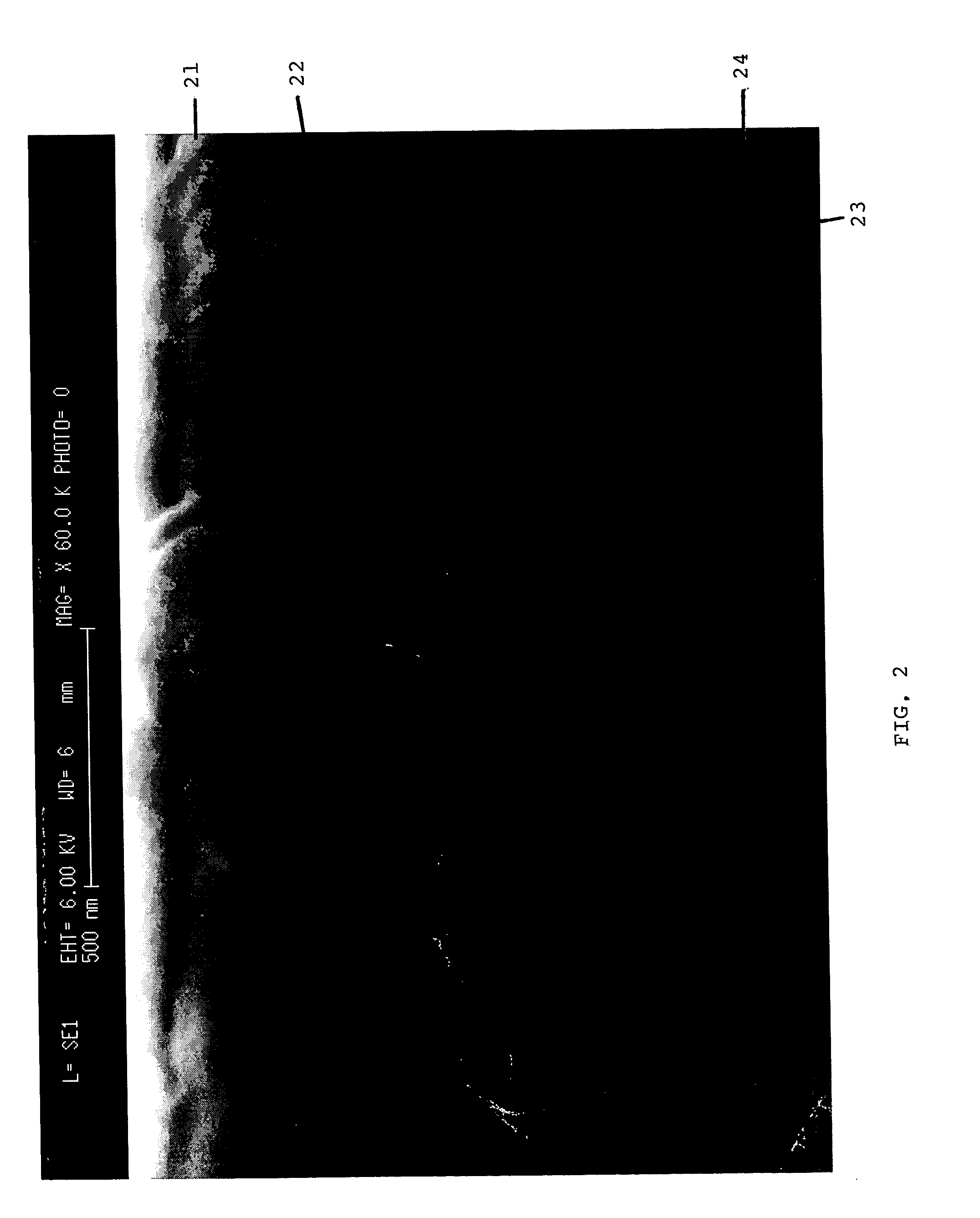
[0026] The present invention relates to a method and apparatus for creating and using a nano-stamp for forming high density elevations, elements or cells on a substrate with nano-scale features including nano-scale-resolution, high-throughput, and potentially low cost. The method of the present invention does not use energetic particles or beams; neither does it require polymer resist to be placed on the surface of a substrate. Instead, the method of the present invention relies on very fast and efficient manufacturing of a nano-stamp by utilizing PVD, CVD, or other surface deposition technique, to produce a two-dimensional nano-scale multi-layered thin film, processing this film into a nano-stamp by cutting it perpendicular to the plane of the layers, atomically polishing the new surface, etching out alternate layers to create alternate elevations, and then indenting a substrate with the grid of alternate elevations under a variety of angles to achieve a desired nano-scale pattern...


PUM

PropertyMeasurementUnit
Lengthaaaaaaaaaa
Angleaaaaaaaaaa
Nanoscale particle sizeaaaaaaaaaa

Abstract

The stamping process and a method of fabrication of nano-stamps with characteristic dimensions below 1 nm and up to 0.1 micron intended for usage in making patterns of characteristic dimensions same as those of the nano-stamp on surface of a substrate is provided. In the process a very hard stamp is fabricated by first depositing alternating layers of two materials, one of which has very high hardness, on some sacrificial substrate via PVD, CVD or any other deposition procedure that produces alternating layers of selected thickness, from sub 1 nm to above 100 nm. The layered film is then polished to atomically smooth finish perpendicular to the plane of the layers and etched to produce dips in the softer layers These steps produce a grid of parallel elevations and valleys on the etched surface, which now can be used as a mold to stamp out patterns on a substrate of lower hardness than the hardness of the elevated layers. If the substrate is stamped twice with turning of the stamp 90 degrees between first and second stampings, a square pattern of hills and valleys is formed, which can be used for magnetic memory storage by subsequently sputtering magnetic material on the tops of the elevations or hills.

Description

[0001] 1. Field of the Invention[0002] The present invention relates to a method for making a nano-stamp and to a method which uses the stamp for producing structured patterns including nano-sized elements on the surface of a substrate for use in nano-scale electronic deviecs, such as integrated circuits (Ics), information storage devices, and photonic and opto-electronic devices, nano-biologic devices, nano-sensors and the like.[0003] 2. Description of the Prior Art[0004] Lithography is the key procedure in industrial manufacturing of numerous small-scale devices, such as the semiconductor-based ICs, micro-electro-mechanical (MEMs) devices, and magnetic, optical, and electro-optical devices. In its well-known form, the process of lithography involves covering a given surface with a plastic material, called a "resist", which has the property of changing its atomic structure under exposure to energetic particles of electromagnetic or other type of radiation (ions, electrons, molecule...

Claims


Application Information

Patent Timeline
IPC IPC(8): G03F7/00
CPCB82Y10/00G03F7/0002B82Y40/00
Inventor PECHENIK, ALEXANDER
Owner PECHENIK ALEXANDER
Why Eureka
Try Eureka