Method for making carbon nanotube-based field emission device

a carbon nanotube and emission device technology, applied in the field of field emission devices, can solve the problems of reducing the uniformity and stability of electron emission from carbon nanotube bundles

Active Publication Date: 2004-10-21
TSINGHUA UNIV +1
View PDF11 Cites 71 Cited by
  • Summary
  • Abstract
  • Description
  • Claims
  • Application Information

AI Technical Summary

Problems solved by technology

All of the above defects may reduce the uniformity and stabili

Method used


Image

  • Method for making carbon nanotube-based field emission device
  • Method for making carbon nanotube-based field emission device
  • Method for making carbon nanotube-based field emission device

Examples


Embodiment Construction

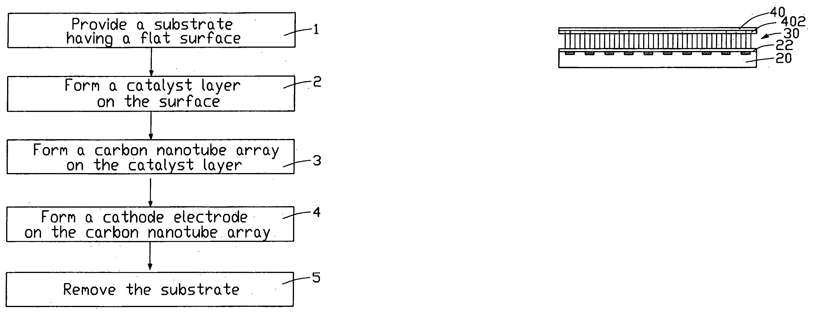
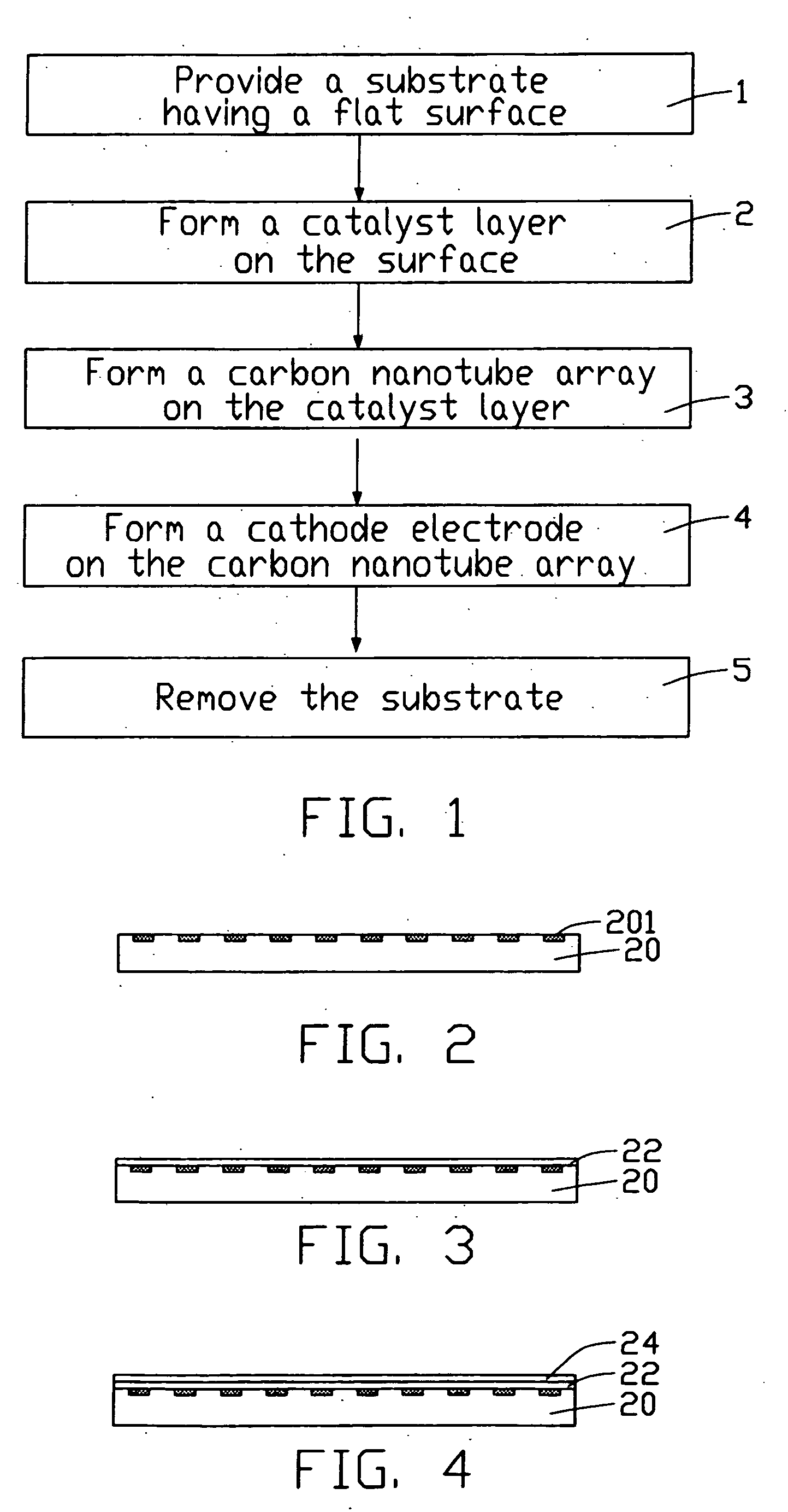
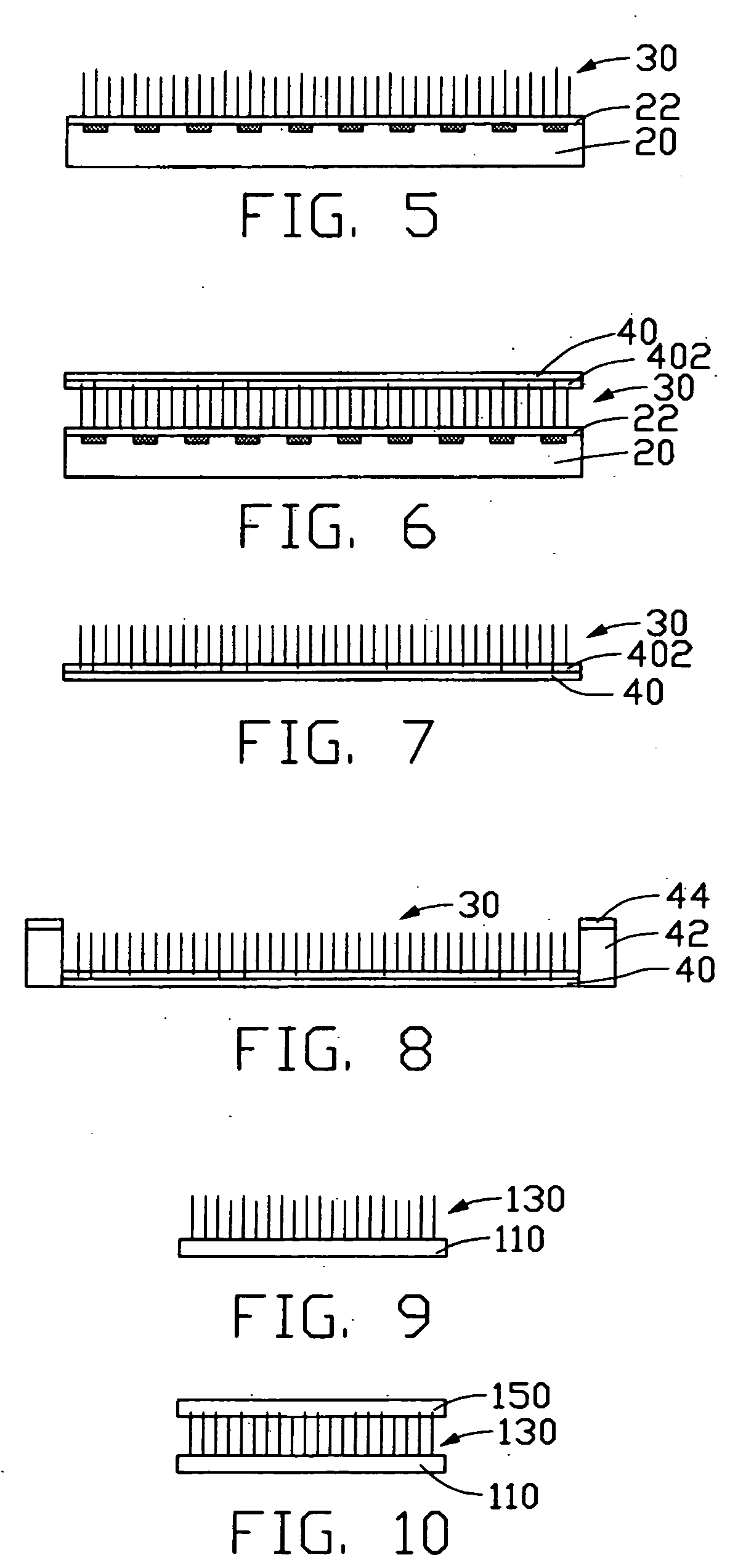
[0022] A preferred method for making a carbon nanotube-based field emission device in accordance with the invention will be described below with reference to FIG. 1.

[0023] Step 1 is providing a substrate having a flat surface. A variation in flatness of the surface is less than 1 micron.

[0024] Step 2 is forming a layer of catalyst on the surface of the substrate. Generally, the catalyst is a transition metal such as Fe (iron), Co (cobalt), Ni (nickel) or an alloy thereof. A thickness of the layer of catalyst is in the range from 1 nm to 10 nm, and preferably in the range from 3 nm to 5 nm. Further, the layer of catalyst is preferably annealed at a temperature of 300.about.400 degree.

[0025] Step 3 is forming a carbon nanotube array on the layer of catalyst. A preferred chemical vapor deposition process for growing the carbon nanotube array includes the following steps: introducing flowing carbon-containing gas such as ethylene or acetylene, heating the flowing carbon-containing gas t...


PUM


Abstract

A preferred method for making a carbon nanotube-based field emission device in accordance with the invention includes the following steps: providing a substrate (22) with a surface; depositing a catalyst layer (24) on a predetermined area on the surface of the substrate; forming a carbon nanotube array (30) extending from the predetermined area; forming a cathode electrode (40) on top of the carbon nanotube array; and removing the substrate so as to expose the carbon nanotube array.

Description

[0001] 1. Field of the Invention[0002] The present invention relates to a method for making a field emission device, and more particularly to a method for making a carbon nanotube-based field emission device.[0003] 2. Description of Prior Art[0004] Carbon nanotubes are a novel carbonaceous material discovered by Iijima, a researcher of NEC corporation, in 1991. Relevant information was reported in an article by Iijima, entitled "Helical Microtubules of Graphitic Carbon" (Nature, Vol.354, P56, 1991). Carbon nanotubes can transmit an extreme high electrical current and emit electrons at a very low voltage of less than 100 volts, which make it a very promising potential material for field emission applications.[0005] Referring to FIG. 12, U.S. Pat. No. 6,232,706, invented by Hongjie Dai et al., discloses a field emission device using aligned parallel bundles of carbon nanotubes 200 extending from patterned catalyst layers 230 deposited on a layer of porous silicon 220 which formed on a...

Claims


Application Information

Patent Timeline
IPC IPC(8): C01B31/02H01J9/02H01L21/00
CPCB82Y10/00B82Y30/00B82Y40/00C01B31/0233C01B2202/08H01J9/025H01J2201/30469C01B32/162
Inventor LIU, LIANGFAN, SHOU SHAN
Owner TSINGHUA UNIV
Why Eureka
Try Eureka