Magnetic random access memory including middle oxide layer and method of manufacturing the same

a random access memory and middle oxide technology, applied in the field of magnetic random access memory, can solve the problems of damage to the interface of thin layers including the lower magnetic layer s1, located under the metal layer, and may aris

Inactive Publication Date: 2004-10-28
SAMSUNG ELECTRONICS CO LTD
View PDF7 Cites 26 Cited by
  • Summary
  • Abstract
  • Description
  • Claims
  • Application Information

AI Technical Summary

Benefits of technology

[0032] A tunneling oxide layer according to the present invention may be formed to have a uniform thickness that can be easily adjusted. As a result, resistance of the MTJ layer may also be easily adjusted and a resistance variation between memory cells may be reduced. In addition, a decrease in MR ratio of an MRAM according to the present invention may be prevented by minimizing or precluding any damage to the lower magnetic layer when forming the tunneling oxide layer.

Problems solved by technology

However, some problems may arise due to the oxidation process of the metal layer.
In particular, when the metal layer is oxidized using the plasma oxidation method, an interface of thin layers including the lower magnetic layer S1, which is located under the metal layer, may be damaged.

Method used


Image

  • Magnetic random access memory including middle oxide layer and method of manufacturing the same
  • Magnetic random access memory including middle oxide layer and method of manufacturing the same
  • Magnetic random access memory including middle oxide layer and method of manufacturing the same

Examples


Embodiment Construction

>

[0073] The MTJ layer of the present invention is formed as shown in FIG. 9 in order to measure characteristics of the MTJ layer such as the MR ratio. In addition, for sake of comparison, an MTJ layer is formed as shown in FIG. 10, i.e., without an oxidation prevention layer.

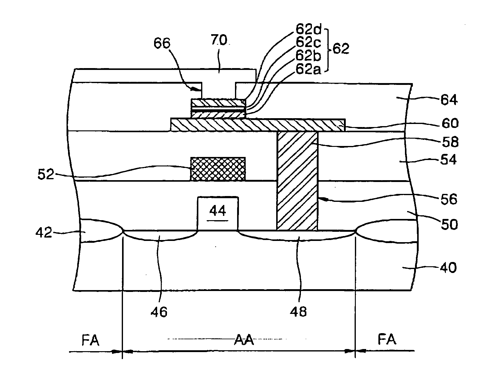
[0074] Referring to FIG. 9, the seed layer 61 in the MTJ layer according to the present invention is formed of a Ta layer using sputtering. The lower magnetic layer 62a, which is a free ferromagnetic layer, is formed of a NiFe layer using sputtering. The oxidation preventing layer 62b and the tunneling oxide layer 62c forming the middle oxide layers are formed of AlO.sub.x layers. The oxidation preventing layer 62b is formed by oxidizing a metal layer, such as aluminum Al, after the metal (Al) layer is formed using a sputtering process, and the tunneling oxide layer 62c is formed by the ALD method. Furthermore, the upper magnetic layer 62d is formed by sequentially stacking a CoFe layer 62d' and an IrMn layer 62...


PUM

PropertyMeasurementUnit
temperatureaaaaaaaaaa

Abstract

In a magnetic random access memory (MRAM) having a transistor and a magnetic tunneling junction (MTJ) layer in a unit cell, the MTJ layer includes a lower magnetic layer, an oxidation preventing layer, a tunneling oxide layer, and an upper magnetic layer, which are sequentially stacked. The tunneling oxide layer may be formed using an atomic layer deposition (ALD) method. At least the oxidation preventing layer may be formed using a method other than the ALD method.

Description

[0001] 1. Field of the Invention[0002] The present invention relates to a semiconductor memory device and a method of manufacturing the same. More particularly, the present invention relates to a magnetic random access memory (MRAM) including a middle oxide layer and an oxidation prevention layer. Further, the present invention relates to a method for providing such an MRAM, and may be a hetero-method.[0003] 2. Description of the Related Art[0004] A magnetic random access memory (MRAM) is a memory device for reading and writing data using a phenomenon that resistance values of a magnetic tunneling junction (MTJ) layer change according to a magnetization direction of two magnetic layers forming the MTJ layer.[0005] An MRAM may be highly integrated and can perform high-speed operations similar to a dynamic random access memory (DRAM) or a synchronous dynamic random access memory (SRAM). An MRAM also has a non-volatile characteristic so that data may be stored for a long time without r...

Claims


Application Information

Patent Timeline
Patent Type & Authority Applications(United States)
IPC IPC(8): B82Y10/00H01L27/105G11C11/15G11C11/16H01F10/32H01F41/30H01L21/8239H01L21/8246H01L43/08
CPCB82Y10/00B82Y25/00B82Y40/00G11C11/16H01F10/3254H01F41/307H01L27/228H10B61/22H10N50/01G11C11/15
Inventor PARK, SANG-JINKIM, TAE-WANLEE, JUNG-HYUNPARK, WAN-JUNSONG, I-HUN
Owner SAMSUNG ELECTRONICS CO LTD
Why Eureka
Try Eureka