Method and apparatus for treating article to be treated

a technology for treating articles and objects, applied in the field of methods and apparatus for processing objects, can solve problems such as difficult to clear the clean room completely, organic contaminants adhesion to the wafer, and deterioration of the characteristics of semiconductor devices

Inactive Publication Date: 2004-11-04
TOKYO ELECTRON LTD
View PDF11 Cites 396 Cited by
  • Summary
  • Abstract
  • Description
  • Claims
  • Application Information

AI Technical Summary

Problems solved by technology

It is difficult to clear the clean room completely of contaminants and the atmosphere of the clean room contains a very small quantity of organic substances (contaminants), such as tributyl phosphate (TBP), a siloxane and dioctyl phthalate (DOP).
Consequently, in some cases, those organic contaminants adhere to the...

Method used


Image

  • Method and apparatus for treating article to be treated
  • Method and apparatus for treating article to be treated
  • Method and apparatus for treating article to be treated

Examples


first embodiment

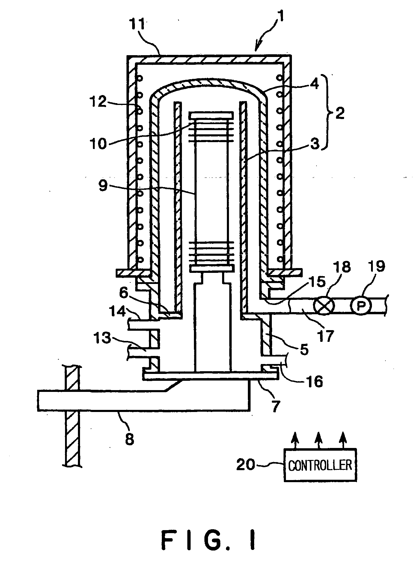
[0088] The thermal treatment apparatus 1 in the first embodiment is capable of removing organic substances from a plurality of wafers 10 held on the wafer boat 9 at one time, and hence many wafers 10 can be cleaned in a short time.

[0089] Possible modifications in the first embodiment will be described.

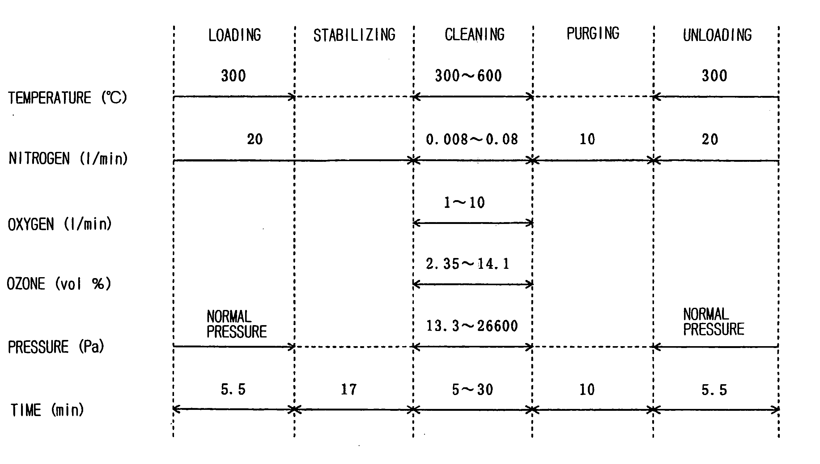
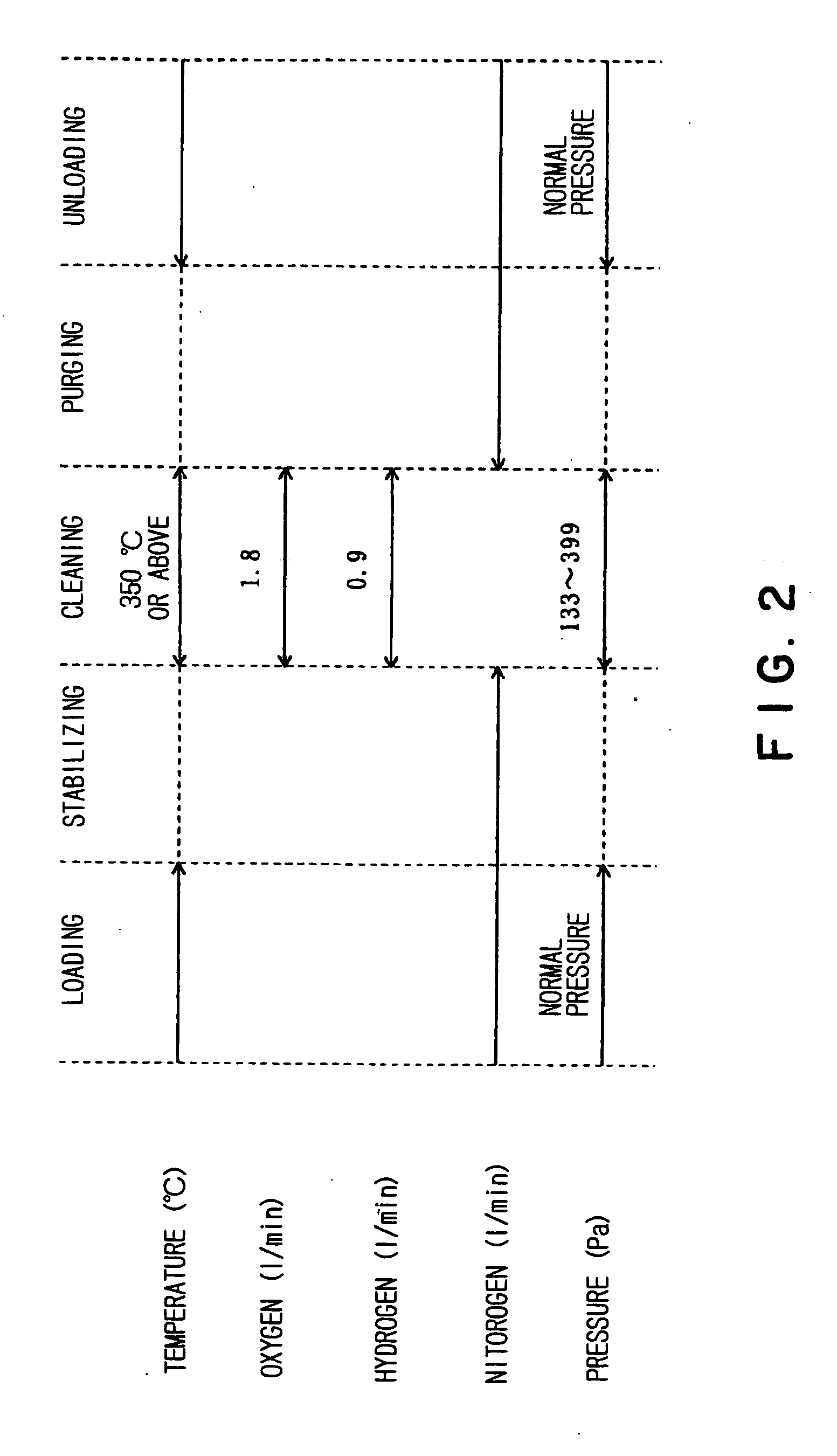
[0090] The first embodiment uses oxygen gas as the oxidizing gas and hydrogen gas as the reducing gas. The oxidizing gas may be at least one of O.sub.2, N.sub.2O and NO, and the reducing gas may be at least one of H.sub.2, NH.sub.3 and CH.sub.4. Organic substances adhering to the wafers 10 can be removed from the wafers 10 by using the active oxygen species and active hydroxyl species produced by the combustion of the reducing gas. The organic substances can be removed from the wafers 10 under the same cleaning conditions including the internal temperature and the internal pressure of the reaction tube 2, when an oxidizing gas other than oxygen gas and a reducing gas other than hydroge...

second embodiment

[0094] A second embodiment of the present invention, in which organic substances adhering to wafers (i.e., objects to be processed) are decomposed and removed therefrom (namely, cleaned) by means of a processing gas containing ozone by using a batch type vertical thermal treatment apparatus shown in FIG. 4, will be described.

[0095] Referring to FIG. 4, the thermal treatment apparatus 101 has a substantially cylindrical reaction vessel 102 set with its axis extending vertically. The reaction vessel 102 is a single-wall cylindrical structure having a top wall. The reaction vessel 102 is formed of a heat-resistant material, such as quartz.

[0096] A cylindrical manifold 103 of a stainless steel is disposed underneath the reaction vessel 102. The manifold 103 is joined in an airtight fashion to the lower end of the reaction vessel 102

[0097] A lid 104 is disposed under the manifold 103. A boat elevator, not shown, moves the lid 104 vertically. The lid 104, the reaction vessel 102 and the m...

third embodiment

[0139] A third embodiment of the present invention, in which organic substances adhering to wafers (i.e., objects to be processed) are decomposed and removed therefrom (namely, cleaned) by means of a processing gas containing ozone, and then silicon dioxide thin films are formed on the cleaned wafers by supplying steam onto the wafers, by using a batch type vertical thermal treatment apparatus shown in FIG. 7, will be described.

[0140] As obvious from FIG. 7, the thermal treatment apparatus 121 is substantially the same in construction as the thermal treatment apparatus 101 in the second embodiment, except that the former is provided additionally with a film-forming gas supply pipe 122 for carrying steam as a film-forming gas to cleaned wafers.

[0141] The film-forming gas supply pipe 122 penetrates the side wall of the manifold 103 into the non-processing region 103c. The film-forming gas supply pipe 122 is connected to a combustor, not shown. The combustor produces steam through the ...


PUM


Abstract

A thermal treatment apparatus 1 includes a reaction tube 2 for containing wafers 10 contaminated with organic substances having a heater 12 capable of heating the reaction tube; a first gas supply pipe 13 for carrying oxygen gas into the reaction tube 2; and a second gas supply pipe 14 for carrying hydrogen gas into the reaction tube 2. Oxygen gas and hydrogen gas are supplied through the first gas supply pipe 13 and the second gas supply pipe 14, respectively, into the reaction tube 2, and the heater 12 heats the reaction tube 2 at a temperature capable of activating oxygen gas and hydrogen gas. A combustion reaction occurs in the reaction tube 2 and thereby the organic substances adhering to the wafers 10 are oxidized, decomposed and removed.

Description

[0001] 1. Field of the Invention[0002] The present invention relates to a method and an apparatus for processing an object to be processed, such as a semiconductor wafer.[0003] 2. Description of the Related Art[0004] A semiconductor device fabricating method, in general, includes a film forming process for forming a thin film, such as a polysilicon film or a silicon oxide film, on an object to be processed, such as a semiconductor wafer (hereinafter, referred to as "wafer") by, for example, CVD (chemical vapor deposition) or the like.[0005] Generally, such a film forming process is carried out in a clean room to prevent the adhesion of contaminants to the wafer. It is difficult to clear the clean room completely of contaminants and the atmosphere of the clean room contains a very small quantity of organic substances (contaminants), such as tributyl phosphate (TBP), a siloxane and dioctyl phthalate (DOP). Consequently, in some cases, those organic contaminants adhere to the wafer. Fo...

Claims


Application Information

Patent Timeline
IPC IPC(8): C30B33/00H01L21/00H01L21/306H01L21/311H01L21/316
CPCC30B33/00H01L21/02046H01L21/02238H01L21/02255H01L21/02301H01L21/02312H01L21/31138H01L21/31662H01L21/67109H01L21/31
Inventor HISHIYA, SHINGOFURUSAWA, YOSHIKAZUHAYASHI, TERUYUKISAITO, MISAKOUMEZAWA, KOTASATO, SYOICHI
Owner TOKYO ELECTRON LTD
Why Eureka
Try Eureka