Detachable substrate with controlled mechanical hold and method for production thereof

a technology of mechanical hold and detachable substrate, which is applied in the direction of microstructural technology, electrical equipment, solid-state devices, etc., can solve the problems of excessive cost of original substrate beneficial to the production of components, inability to transfer to another support, and inability to meet the requirements of production

Inactive Publication Date: 2004-11-11
COMMISSARIAT A LENERGIE ATOMIQUE ET AUX ENERGIES ALTERNATIVES
View PDF26 Cites 103 Cited by
  • Summary
  • Abstract
  • Description
  • Claims
  • Application Information

AI Technical Summary

Problems solved by technology

However, a highly resistive substrate is not necessarily available at the same cost and with the same quality as the standard substrates usually employed.
There may also be cited situations in which the original substrate that is beneficial for the production of the components is excessively costly.
In some cases the transfer to another support is not indispensable, especially if the final thickness aimed at during thinning is sufficient to produce self-supporting structures.
A problem then arises in choosing the means employed to assemble the layer and the substrate.
More generally, the problem that arises is that of assembling a wafer with another wafer, which wafers can be substrates, thin layers, or sufficiently thick to be self-supporting, composite or otherwise, composed of at least one or more semiconductor materials, partly, completely processed or unprocesse

Method used


Image

  • Detachable substrate with controlled mechanical hold and method for production thereof
  • Detachable substrate with controlled mechanical hold and method for production thereof
  • Detachable substrate with controlled mechanical hold and method for production thereof

Examples


Embodiment Construction

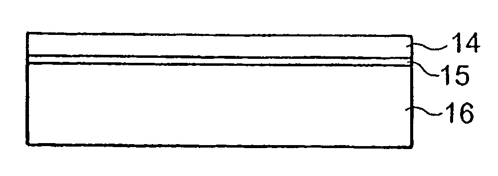
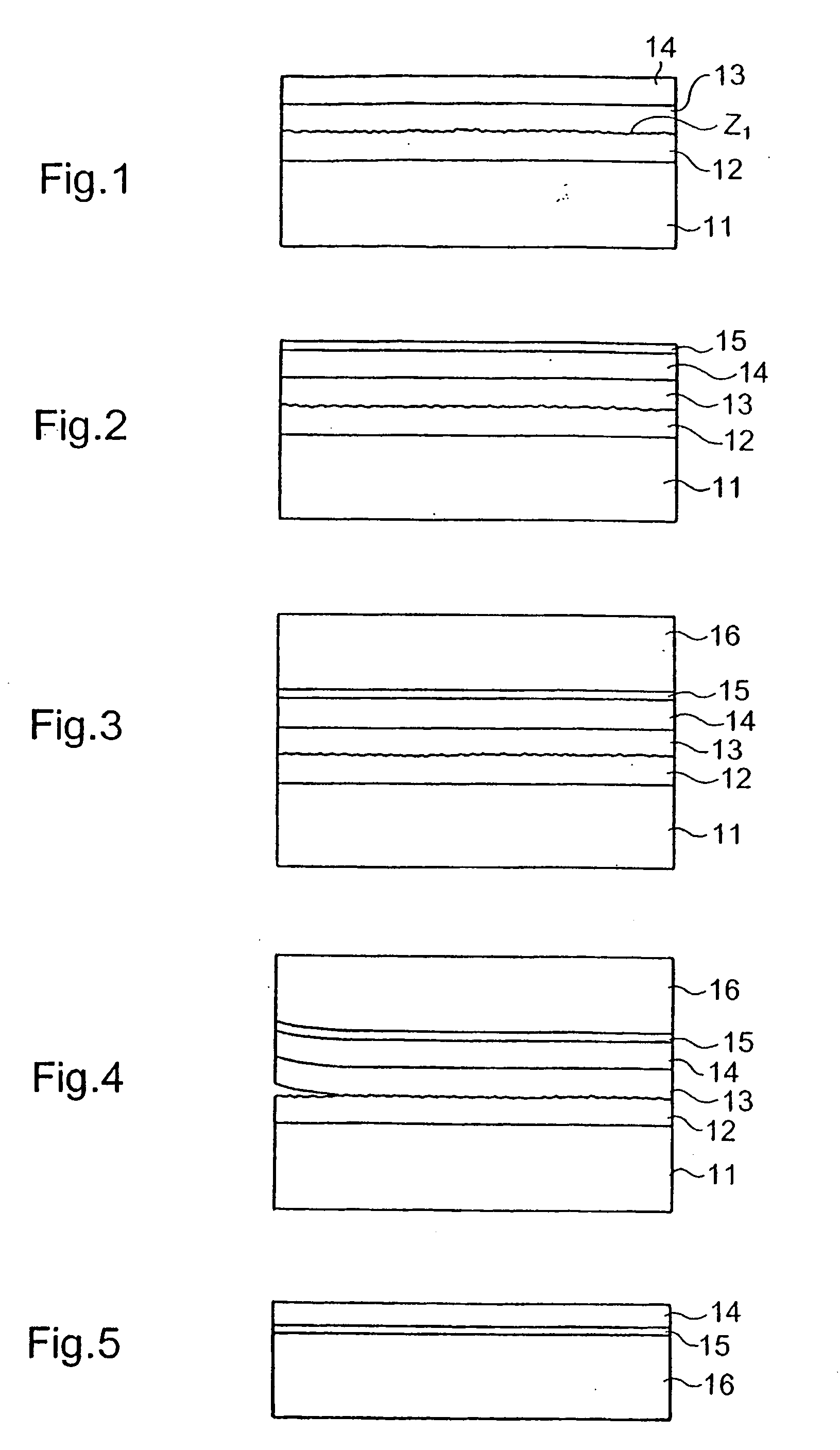
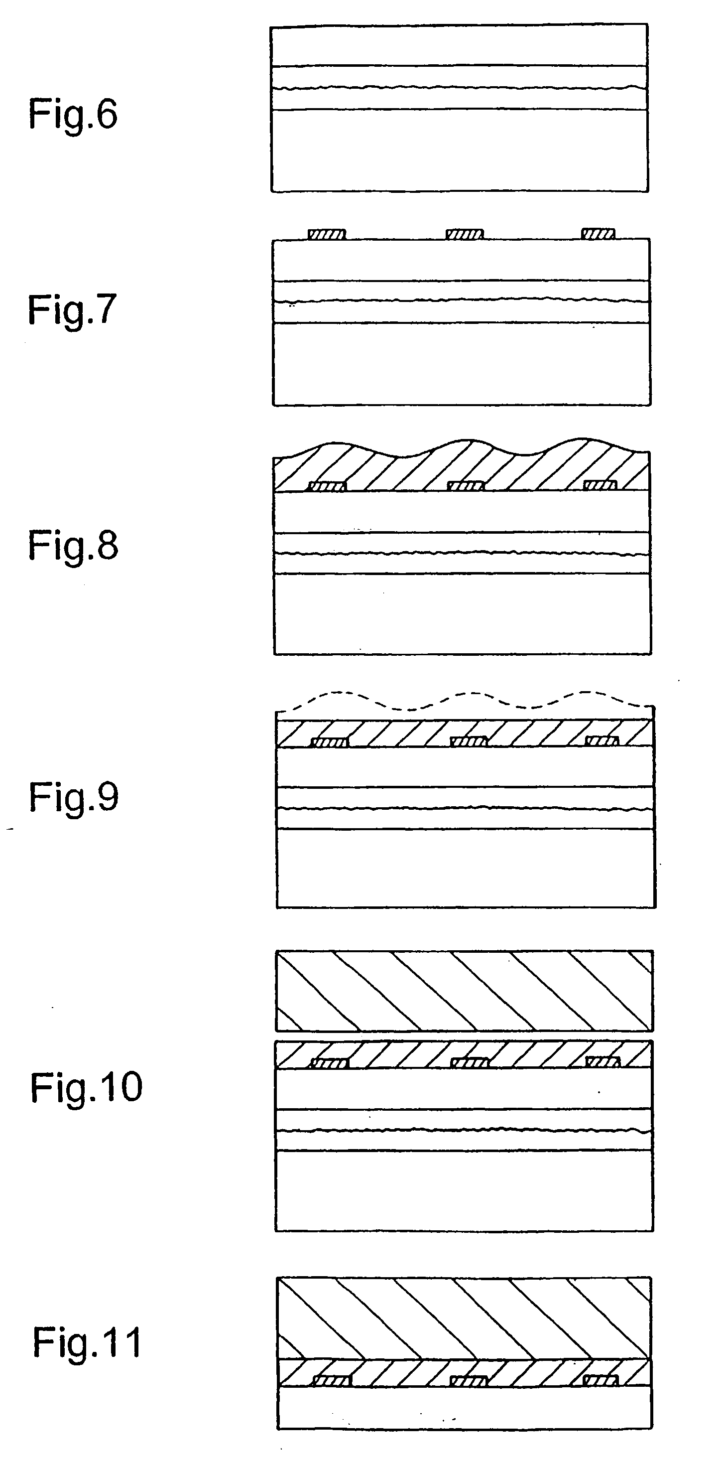
[0075] The preferred examples selected for the detailed description primarily relate to silicon, which is generally available in the form of round substrates, for example of 200 mm diameter. These methods transfer readily to other systems characterized in particular by materials other than silicon, in a nonlimiting manner and without departing from the scope of the invention.

[0076] Some embodiments of the method according to the invention tend to encourage lifting of the layer off its substrate at the overall level, i.e. on the scale of the whole of the substrate, while others tend to lift off delimited fragments.

[0077] For producing a detachable SOI substrate, examples of SiO.sub.2 / SiO.sub.2 and Si / SiO.sub.2 bonding are considered. In the case of layers of different kinds (Si.sub.3N.sub.4 is another conventional example, but there are also silicides), and by analogy with what is described hereinafter, it suffices to use appropriate chemical treatment (for example NH.sub.4OH / H.sub.2...


PUM


Abstract

The invention relates to a method for production of a detachable substrate, comprising a method step for the production of an interface by means of fixing, using molecular adhesion, one face of a layer on one face of a substrate, in which, before fixing, a treatment stage for at least one of said faces is provided, rendering the mechanical hold at the interface at such a controlled level to be compatible with a subsequent detachment.

Description

[0001] The invention relates to a method of assembling two micro-electronic wafers and the resulting structure. It finds applications in the fabrication of thin layer substrates and in transferring layers or components onto supports of any kind.DESCRIPTION OF THE PRIOR ART[0002] Increasingly, components must be integrated onto supports different from those used to produce them.[0003] Components on plastics material substrates or on flexible substrates may be cited, for example. By component is meant any micro-electronic, opto-electronic or sensor (for example chemical, mechanical, thermal, biological or biochemical sensor) device that is completely or partly "processed", i.e. completely or partly produced.[0004] A layer transfer method can be used to integrate the components onto flexible supports.[0005] There are many other examples of applications in which layer transfer techniques can provide a suitable solution for integrating components or layers onto a support that is a priori...

Claims


Application Information

Patent Timeline
IPC IPC(8): B81C99/00H01L21/02H01L21/762H01L27/12
CPCB81C99/008H01L21/76254Y10S438/958H01L21/20
Inventor ASPAR, BERNARDMORICEAU, HUBERTRAYSSAC, OLIVIERGHYSELEN, BRUNO
Owner COMMISSARIAT A LENERGIE ATOMIQUE ET AUX ENERGIES ALTERNATIVES
Why Eureka
Try Eureka