Transmitter circuit, transmission circuit and driver unit

a transmission circuit and driver unit technology, applied in the field of transmission circuits and transmission circuits, can solve the problems of inability to achieve good signal transmission and significant blunting of signal waveform at the input end of the receiver circuit, and achieve the effect of reducing the size, weight and cost of display devices

Inactive Publication Date: 2004-12-02
RENESAS ELECTRONICS CORP
View PDF10 Cites 37 Cited by
  • Summary
  • Abstract
  • Description
  • Claims
  • Application Information

AI Technical Summary

Benefits of technology

0006] For the purpose of reducing the size, weight and cost of display devices, progress has recently been made in COG (Chip On Glass) techniques for mounting a source driver LSI chip on a glass substrate such as a matrix display panel. In such an arrangement, transmission

Problems solved by technology

Consequently, even if signal transmission is performed in a high-frequency region that exceeds 100 MHz with the higher resolutions and larger screen areas of display panels, the signal w

Method used


Image

  • Transmitter circuit, transmission circuit and driver unit
  • Transmitter circuit, transmission circuit and driver unit
  • Transmitter circuit, transmission circuit and driver unit

Examples


first embodiment

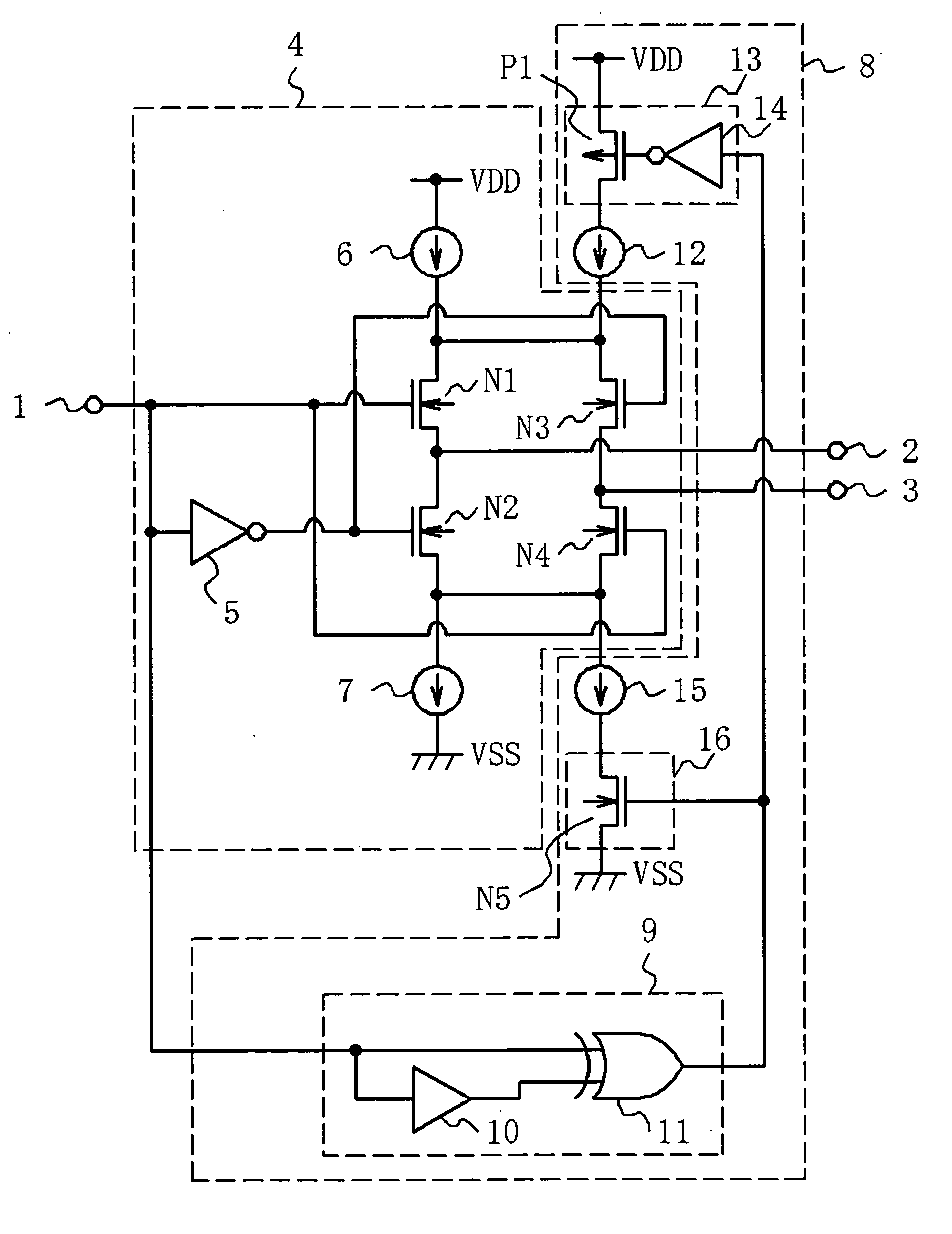
[0033] FIG. 1 is a diagram illustrating a configuration of a transmitter circuit according to the present invention. As shown in FIG. 1, the transmitter circuit includes an input terminal 1, a non-inverting output terminal 2, an inverting output terminal 3, a driver circuit 4 and an output-waveform control circuit 8.

[0034] The driver circuit 4 includes a CMOS-type inverter circuit 5, a constant-current source 6 for signal current source, a constant-current source 7 for signal current sink, and N-channel MOS transistors N1, N2, N3 and N4. One end of the constant-current source 6 is connected to a high-potential power supply VDD and the other end thereof is connected to the drain terminal of the N-channel MOS transistor N1 and to the drain terminal of the N-channel MOS transistor N3. One end of the constant-current source 7 is connected to a low-potential power supply VSS and the other end thereof is connected to the source terminal of the N-channel MOS transistor N2 and to the source...

second embodiment

[0052] As shown in FIG. 4, the transmitter circuit includes the input terminal 1, non-inverting output terminal 2, inverting output terminal 3, driver circuit 4 and output-waveform control circuit 17.

[0053] The output-waveform control circuit 17 includes CMOS-type inverter circuits 18 and 20 and capacitors 19 and 21. The input terminal of the inverter circuit 20 is connected to the input terminal 1 and has the non-inverted input data signal applied thereto. One end of the capacitor 21 is connected to the output terminal of the inverter circuit 20 and the other end of the capacitor 21 is connected to the inverting output terminal 3. The input terminal of the inverter circuit 18 is connected to the output terminal of the inverter circuit 5 and has the inverted input data signal applied thereto. One end of the capacitor 19 is connected to the output terminal of the inverter circuit 18 and the other end of the capacitor 19 is connected to the non-inverting output terminal 2.

[0054] The ...

fourth embodiment

[0087] As shown in FIG. 8, the transmitter circuit includes the input terminal 1, non-inverting output terminal 2, inverting output terminal 3, driver circuit 22 and output-waveform control circuit 17.

[0088] In accordance with the transmitter circuit of the fourth embodiment, as described above, effects similar to these of the third embodiment are obtained by circuitry of a scale smaller than that of the transmitter circuit of the third embodiment.


PUM


Abstract

A transmitter circuit for use in a display device of the type having a transmission line consisting of aluminum or copper conductor formed on a glass substrate includes a driver circuit, which has a non-inverting output terminal and an inverting output terminal, for outputting a signal current, which has a loop direction that changes based upon an input signal, to the non-inverting and inverting output terminals; and an output-waveform control circuit for detecting the edge of the waveform of the input signal and responding by increasing the signal current temporarily.

Description

[0001] This invention relates to a transmitter circuit, a transmission circuit and a driver unit. More particularly, the invention relates to a transmitter circuit, a transmission circuit and a driver unit applicable to a liquid crystal display device, an organic electroluminescence display device and a plasma display device.[0002] Conventionally, in a matrix-type liquid crystal display device, an organic electroluminescence (EL) display device and a plasma display device, a timing controller LSI chip, which successively generates and outputs one horizontal line of a grayscale data signal and scanning signal from one frame of image signals, and a source driver LSI chip, which serves as a driver unit that receive the grayscale data signal and drive respective ones of data lines of a display panel, are mounted on a printed circuit board. Transmission of signals between the timing controller LSI chip and the source driver LSI chip, as well as transmission of signals between the source ...

Claims


Application Information

Patent Timeline
IPC IPC(8): G09G3/20H03F3/16H03K5/1534H03K17/687H03K19/0175H04L25/02
CPCG09G3/20G09G2310/0267G09G2310/0275G09G2370/08H03K5/1534H04L25/0272H04L25/0286
Inventor HOSOKAWA, AKIONISHIMURA, KOUICHI
Owner RENESAS ELECTRONICS CORP
Why Eureka
Try Eureka