

Lithographic processing method and device manufactured thereby
a technology of lithographic processing and device, applied in the field of lithographic equipment, can solve the problems of inability to produce device layers with 90 nm contact holes at minimum and larger pitches, and the depth of focus and insensitivity to residual errors in the exposure dose of irradiated target portions become small,
- Summary
- Abstract
- Description
- Claims
- Application Information
AI Technical Summary
Benefits of technology
Problems solved by technology
Method used
Image

Examples
embodiment 1
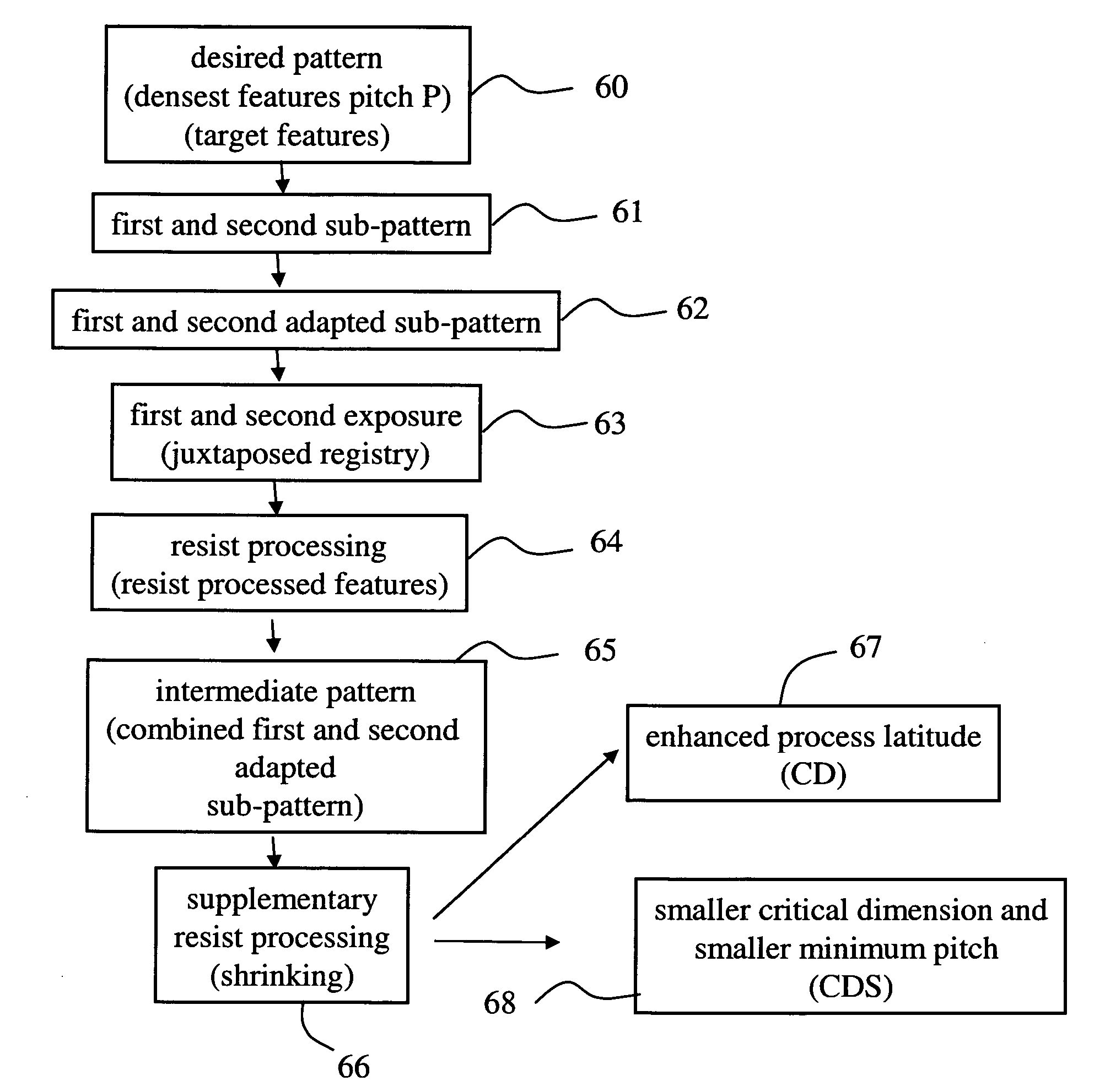
[0063] Embodiment 1
[0064] The method according to the present invention is schematically indicated in FIG. 5. Data defining a desired pattern having densest features at a pitch P is used as input information 60 for separating the pattern into a first and second sub-pattern 61, for example in terms of a data set on a data carrier for use with a computer. Commercially available mask pattern design check rule tooling can be used for splitting the pattern into the sub-patterns, whereby the minimum pitches occurring in the sub-patterns are larger than P. Next, the data 61 are adapted such as to provide corresponding adapted sub-pattern data 62 whereby the features of the sub-patterns are expanded in size. Typically, the expansion corresponds to a preselected dilatation distance of the edges of the features, substantially independent of the nominal size of a feature. Therefore, in general, the expansion is not expressible as a single magnification factor to be applied to the features, unl...
embodiment 2
[0073] Embodiment 2
[0074] An embodiment according to the present invention whereby the method is fully exploited to obtain a reduction of critical dimension (such as indicated by element 68 of FIG. 5) which can be processed in combination with a reduction of the minimum pitch for arrangements of such critical dimension sized features (i.e., the minimum pitch at which such an arrangement of contact holes can be patterned in the resist layer), is illustrated in FIGS. 6 and 7. A desired device pattern comprises dense contact holes 74 arranged in a honeycomb pattern of which a set of two unit cells 70 is shown in FIG. 6. The device pattern may further comprise isolated contact holes not shown in FIG. 6. The desired contact holes 74 occur at a minimum pitch P represented by arrow 75 in FIG. 6, which is twice the diameter of a single contact hole 74.
[0075] With the present embodiment, the method is used on a lithographic apparatus provided with a phase shift mask, however, even under opti...
embodiment 3
[0078] Embodiment 3
[0079] An embodiment according to the present invention is the same as embodiment 1 or 2, whereby attenuating PSM's with attenuating phase shift absorbers between sub-pattern features are used to enhance the process window.
[0080] Generally, attenuating PSM's feature an additional chrome shielding of attenuated absorber areas to enhance aerial image contrast. With the present method such an additional chrome shielding of attenuated absorber areas of each of the sub patterns is not needed. It has been verified that in a double exposure process according to the invention any background radiation passing an attenuating absorber between two bright contact holes or short trenches as present in a sub-pattern, not substantially degrades the aerial image contrast.
PUM
 Abstract
Description
Claims
Application Information