Corrosion-resistant copper bond pad and integrated device

a technology of copper bond pad and integrated device, which is applied in the direction of fluid pressure measurement, fluid pressure measurement by electric/magnetic elements, instruments, etc., can solve the problems of aluminum bond pad being susceptible to corrosion under standard environmental test conditions, product failure, performance degradation and other issues

Inactive Publication Date: 2005-01-06
NORTH STAR INNOVATIONS
View PDF10 Cites 81 Cited by
  • Summary
  • Abstract
  • Description
  • Claims
  • Application Information

AI Technical Summary

Problems solved by technology

These bond pads need to be protected from environmental conditions such as high humidity, which are known to degrade the performance of an electronics assembly.
Bond pads are often made of aluminum because aluminum or gold bond wires are readily attached to the bond pads, yet the aluminum bond pads are susceptible to corrosion under standard environmental test conditions.
This corrosion can cause performance degradation and product failure when the joint between a gold wire and an aluminum pad degrades and fails.
Unfortunately, dispensing and curing the silicone is a time-consuming process.
The silicone, having a higher dielectric constant and loss tangent than air, may cause a degradation of high-frequency and radio-frequency (RF) performance.
In addition, silicone encapsulations are difficult to remove completely, precluding rework and repair.
Unfortunately, fluorosilicones can degrade RF performance of RF devices operating at high frequencies and can be difficult to remove.
The film or coating, which is vacuum-deposited, cannot be used with chip-on-board (COB) applications and is an expensive process, particularly when applied at the assembled device level.
This approach does not address the RF performance and repairability problems for COB applications.
While this approach is effective, it is not compatible with chip-on-board assembly applications and adds bulk.
This more complex process is incompatible with MEMS sensing requirements and does not address the RF performance degradation problem for COB applications.
The copper surface of copper bond pads are generally not suitable as a terminal metal for packaging interconnections, and as a result, some manufacturers have coated the pads with other deposited metals such as palladium and nickel to reduce or eliminate voids in the copper or at the interface between the copper and the nickel.
In addition, such a method would result in circuits, sensors and assemblies that do not require a complex cleaning process, have repairable and reworkable bond pads, have improved reliability of electrical connections to the integrated circuits, and do not have degraded RF performance.

Method used


Image

  • Corrosion-resistant copper bond pad and integrated device
  • Corrosion-resistant copper bond pad and integrated device
  • Corrosion-resistant copper bond pad and integrated device

Examples


Embodiment Construction

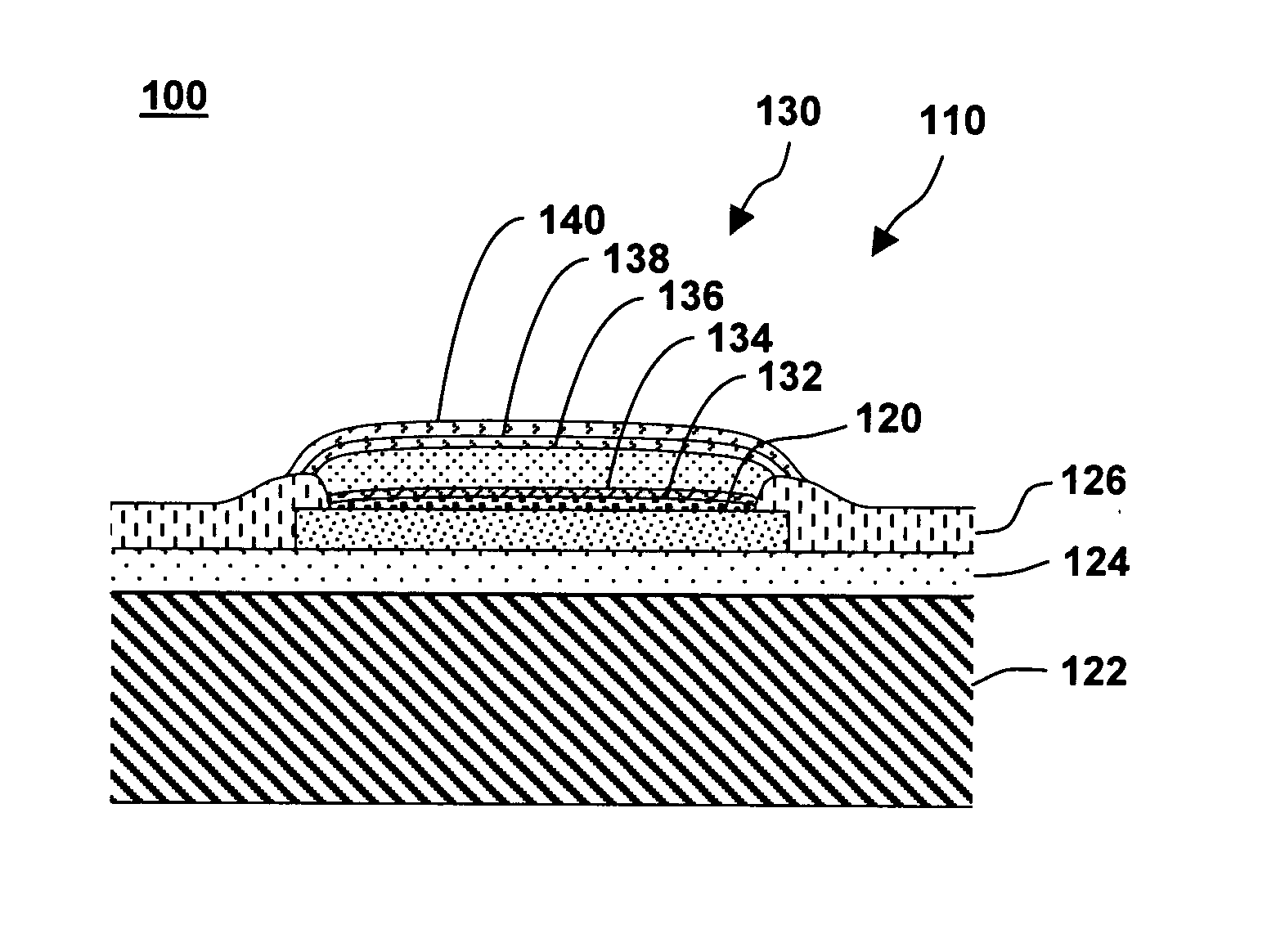
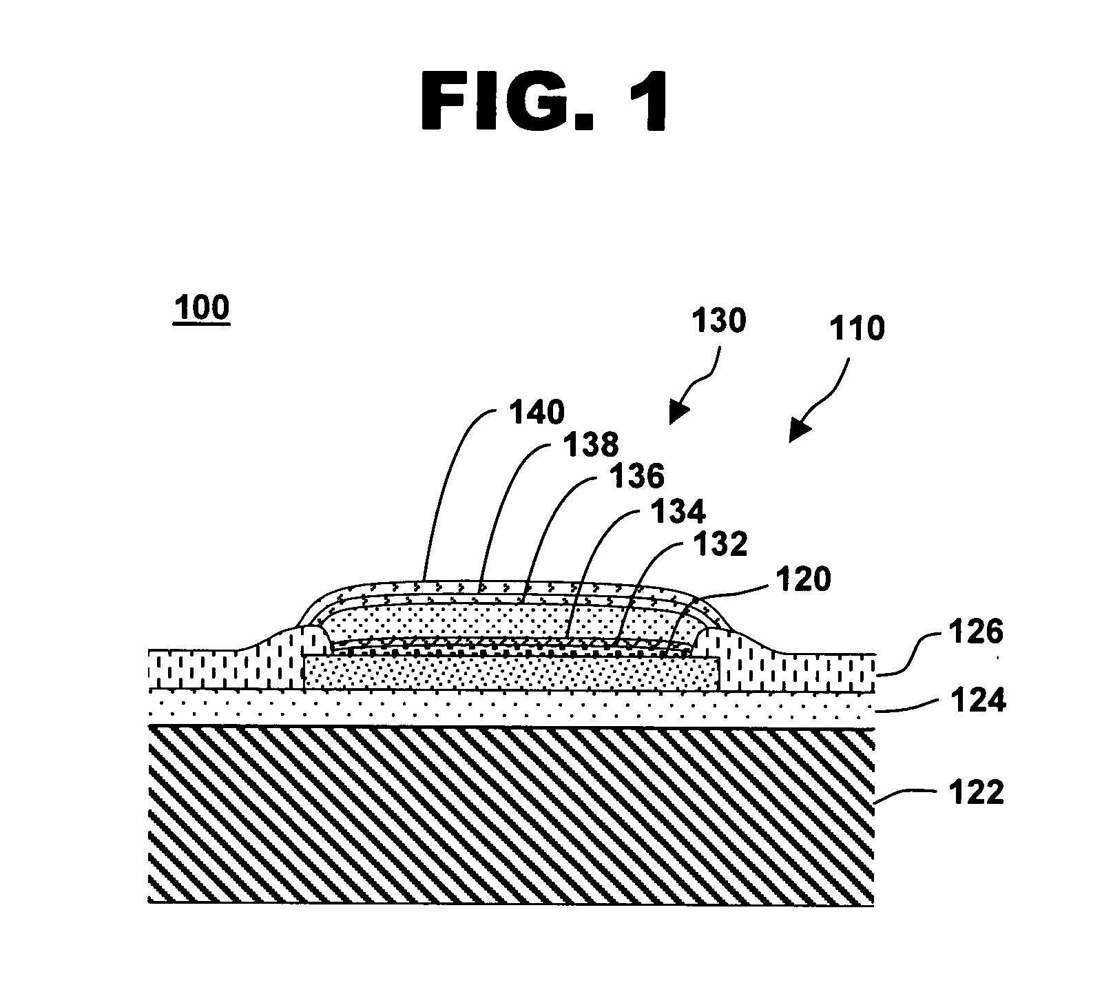
[0024]FIG. 1 shows a cross-sectional cutaway view of a capped copper bond pad on an integrated device, in accordance with one embodiment of the present invention at 100. Capped copper bond pads 130 are typically located on the surface of an integrated device 110. Capped copper bond pads 130 provide for wirebonding and electrical connections between capped copper bond pads 130 and a package or assembly to which integrated device 110 is electrically connected, such as a plastic package, a ceramic package, or a sensor package. Capped copper bond pads 130 can be wirebonded to provide electrical connectivity between integrated device 110 and external power supplies, ground lines, input signals, output signals, data lines, address lines, other integrated devices, external electronic components, and other electrical and electronic devices. Integrated device 110 typically includes a plurality of capped copper bond pads 130. Integrated device 110 with capped copper bond pads 130 may be conta...


PUM

PropertyMeasurementUnit
thicknessaaaaaaaaaa
thicknessaaaaaaaaaa
thicknessaaaaaaaaaa

Abstract

The invention provides an integrated device with corrosion-resistant capped copper bond pads. The capped copper bond pads include at least one copper bond pad on a semiconductor substrate. An activation layer comprising one of immersion palladium, electroless cobalt, or immersion ruthernium is disposed on the copper bond pad. A first intermediate layer of electroless nickel-boron alloy is disposed on the activation layer. A second intermediate layer comprising one of electroless nickel or electroless palladium is disposed on the first intermediate layer, and an immersion gold layer is disposed on the second intermediate layer. A capped copper bond pad and a method of forming the capped copper bond pads are also disclosed.

Description

FIELD OF THE INVENTION [0001] This invention relates generally to semiconductor processing. More specifically, the invention relates to a corrosion-resistant capped copper bond pad for integrated circuits and sensors, and methods of forming the capped copper bond pad at the wafer, die and assembly level. BACKGROUND OF THE INVENTION [0002] Electronics assembly applications such as integrated circuits and silicon-based sensors generally include multiple layers of metal traces that terminate in metal bond pads through which electrical signals are transmitted. These bond pads need to be protected from environmental conditions such as high humidity, which are known to degrade the performance of an electronics assembly. [0003] Bond pads are often made of aluminum because aluminum or gold bond wires are readily attached to the bond pads, yet the aluminum bond pads are susceptible to corrosion under standard environmental test conditions. This corrosion can cause performance degradation and...

Claims


Application Information

Patent Timeline
Patent Type & Authority Applications(United States)
IPC IPC(8): G01L9/00H01L21/60H01L23/485H01L23/498
CPCG01L19/0069G01L19/147H01L23/498H01L24/05H01L24/11H01L24/12H01L24/45H01L24/48H01L2224/0401H01L2224/04042H01L2224/05147H01L2224/05155H01L2224/05164H01L2224/05644H01L2224/13099H01L2224/13109H01L2224/45124H01L2224/45144H01L2224/48091H01L2224/48227H01L2224/48465H01L2224/48699H01L2224/85013H01L2924/01005H01L2924/01006H01L2924/01011H01L2924/01013H01L2924/01014H01L2924/01015H01L2924/01022H01L2924/01027H01L2924/01028H01L2924/01029H01L2924/01046H01L2924/01047H01L2924/01049H01L2924/0105H01L2924/01073H01L2924/01074H01L2924/01075H01L2924/01078H01L2924/01079H01L2924/01082H01L2924/01083H01L2924/01327H01L2924/014H01L2924/04941H01L2924/04953H01L2924/05042H01L2924/09701H01L2924/14H01L2924/19041H01L2924/3025H01L2224/32225H01L2224/73265H01L2924/01033H01L2924/01044H01L2224/48644H01L2924/10253H01L2924/00014H01L2924/00H01L2224/48744H01L2924/181H01L2924/00012
Inventor DUNN, GREGORY J.FAY, OWEN R.DEAN, TIMOTHY B.BLAKE, TERANCECHELINI, REMY J.LYTLE, WILLIAM H.STRUMBERGER, GEORGE A.
Owner NORTH STAR INNOVATIONS
Why Eureka
Try Eureka