Electroless surface treatment plated layers of printed circuit board and method for preparing the same

a surface treatment technology, which is applied in the direction of resistive material coating, metallic pattern materials, solid-state devices, etc., can solve the problems of electrical characteristics deterioration, problems of surface treatment technology of printed circuit board according to the related art,

Active Publication Date: 2013-01-03
SAMSUNG ELECTRO MECHANICS CO LTD
View PDF11 Cites 19 Cited by
  • Summary
  • Abstract
  • Description
  • Claims
  • Application Information

AI Technical Summary

Benefits of technology

[0013]An object of the present invention is to provide an electroless surface treatment plated layer of a printed circuit board capable of solving a non-uniformity problem of current flow caused by a skin effect by solving several problems generated due to a thick thickness of a nickel layer included in a plated layer in connecting the surface treatment plated layer and external devices to each other using a wire bonding scheme.

Problems solved by technology

However, in accordance with miniaturization of a wiring for increasing density of the electronic component, problems of a technology of surface-treating the circuit board according to the related art have started to emerge.
However, the Ni layer has electrical resistance higher than that of Cu, such that electrical characteristics are deteriorated.
The reason is that when the space between the patterns becomes narrow, the Ni layer abnormally grows between the patterns to thereby cause an electrical bridge.

Method used


Image

  • Electroless surface treatment plated layers of printed circuit board and method for preparing the same
  • Electroless surface treatment plated layers of printed circuit board and method for preparing the same
  • Electroless surface treatment plated layers of printed circuit board and method for preparing the same

Examples


example 1

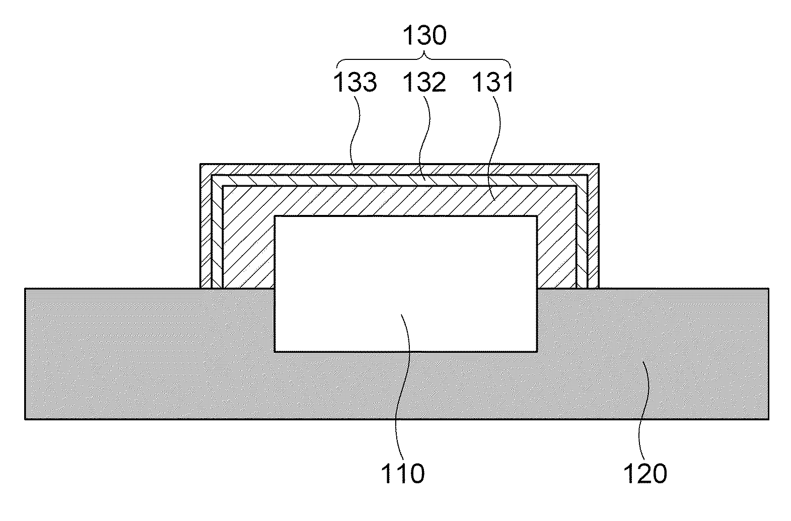
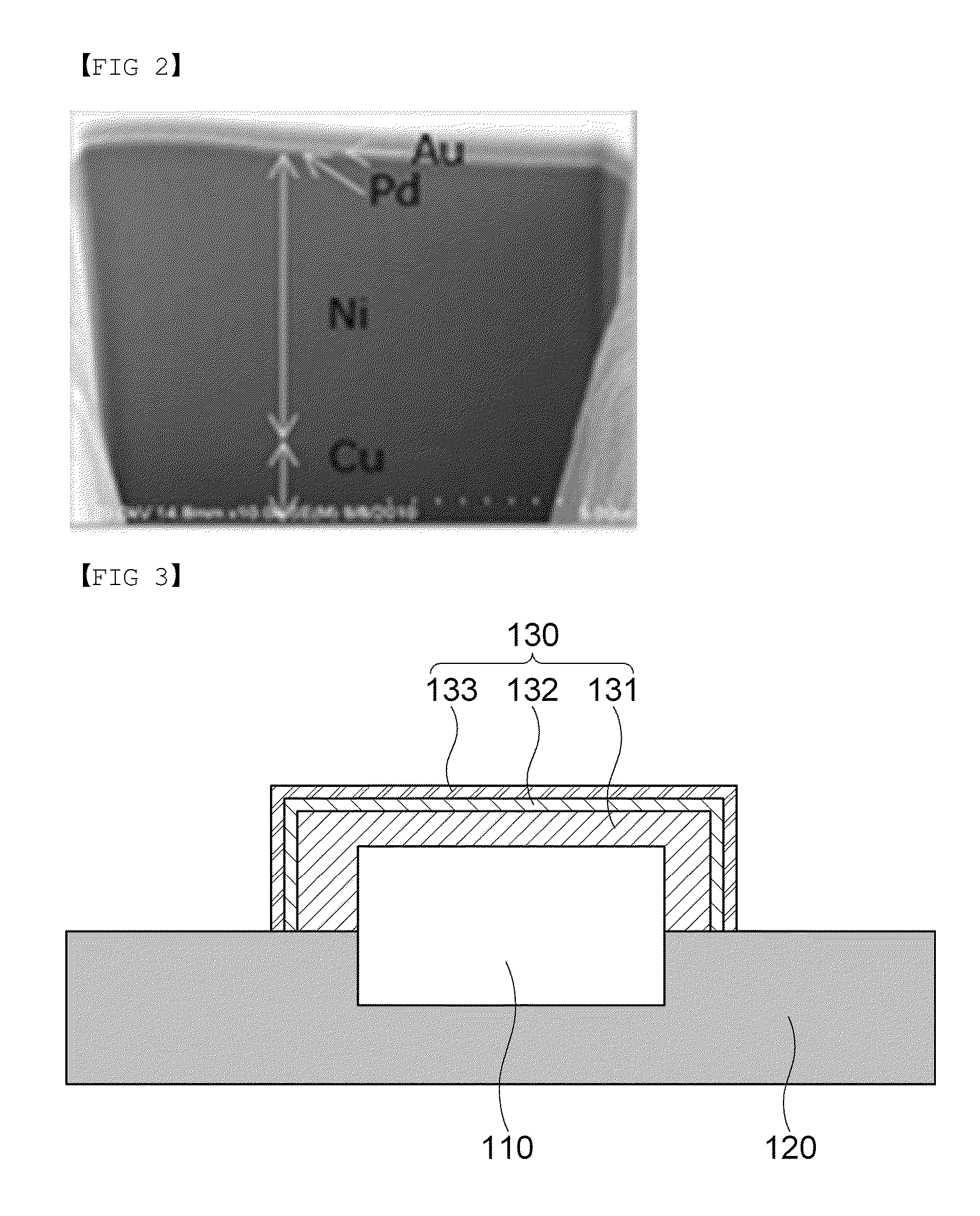
[0053]1) Electroless Ni Plating

[0054]A substrate subjected to pretreatment was immersed in an electroless Ni plating solution (pH: 4.2 to 4.4, NPR-4: a product available from Uyemora & Co., Ltd) allowing 10 wt % of phosphorus to be contained in a plated coating at a temperature of 65° C. for 1 minute and then cleaned for 2 minutes to thereby obtain an electroless nickel plated coating having a thickness of 0.1 μm.

[0055]2) Electroless Pd Plating

[0056]The substrate subjected to the electroless Ni plating was immersed in XTP (pH: 7.2, a product available from Uyemora & Co., Ltd), which is an electroless Pd plating solution, at a temperature of 50° C. for 10 minutes and then cleaned for 2 minutes to thereby obtain an electroless palladium plated coating having a thickness of 0.1 μm.

[0057]3) Electroless Au Plating

[0058]The substrate subjected to the electroless Ni plating and the electroless Pd plating was immersed in an electroless gold plating solution (GoBright TSB-72, a product avail...

experimental example

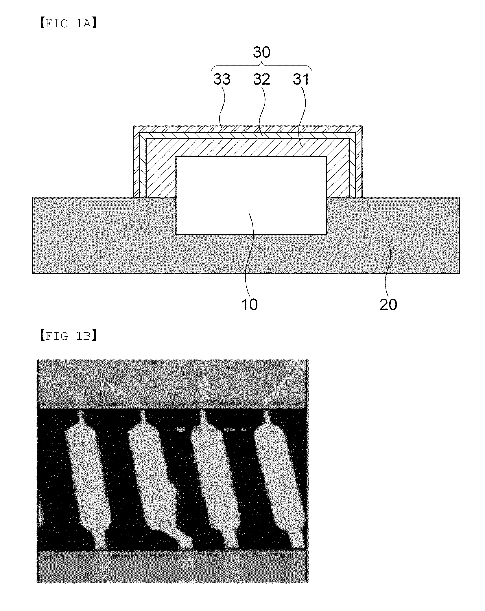
[0062]Cross-sectional photographs of the electroless nickel / palladium / gold plated layers obtained according to Example and Comparative Example were observed by a scanning electron microscope (SEM). Results of the observation were shown in FIGS. 2 and 4.

[0063]Referring to FIG. 2, in the case of the nickel / palladium / gold plated layer according to the related art, it may be appreciated that the nickel plated coating has a significant thick thickness. In this case, a current flows in the nickel layer of the plated layer while mainly flowing along a surface in a high frequency band, thereby causing a problem that electrical resistance increases due to a skin effect in which the current mainly flows in the nickel layer rather than an inner layer of copper wiring.

[0064]However, referring to FIG. 4 showing a cross-sectional photograph of the electroless nickel / palladium / gold surface treatment plated layer prepared according to the exemplary embodiment of the present invention, it may be app...


PUM

PropertyMeasurementUnit
thicknessaaaaaaaaaa
thicknessaaaaaaaaaa
thicknessaaaaaaaaaa

Abstract

Disclosed herein are an electroless surface treatment plated layer of a printed circuit board, a method for preparing the same, and printed circuit board including the same. The electroless surface treatment plated layer includes: electroless nickel (Ni) plated coating/palladium (Pd) plated coating/gold (Au) plated coating, wherein each of the electroless nickel, palladium, and gold plated coatings has a thickness of 0.02 to 1 μm, 0.01 to 0.3 μm, and 0.01 to 0.5 μm. In the electroless surface treatment plated layer of the printed circuit board, a thickness of the nickel plated coating is specially minimized to 0.02 to 1 μm, thereby making it possible to form an optimized electroless Ni/Pd/Au surface treatment plated layer.

Description

CROSS REFERENCE(S) TO RELATED APPLICATIONS[0001]This application claims the benefit under 35 U.S.C. Section 119 of Korean Patent Application Serial No. 10-2011-0062940, entitled “Electroless Surface Treatment Plated Layers of Printed Circuit Board and Method for Preparing the Same” filed on Jun. 28, 2011, which is hereby incorporated by reference in its entirety into this application.BACKGROUND OF THE INVENTION[0002]1. Technical Field[0003]The present invention relates to an electroless surface treatment plated layer of a printed circuit board, a method for preparing the same, and a printed circuit board including the same.[0004]2. Description of the Related Art[0005]In accordance with an increase in density of an electronic component, various technologies regarding surface treatment of a printed circuit board (PCB) have been developed. In accordance with the recent demand of PCB products that have been thinned and densified, a process of treating a surface of the PCB has been recen...

Claims


Application Information

Patent Timeline
Patent Type & Authority Applications(United States)
IPC IPC(8): H05K7/00H05K1/09B32B15/01H05K3/00
CPCH05K1/09H05K7/00H05K1/0216H05K3/244H05K2201/0338Y10T428/12889C23C18/32C23C18/54B32B15/018C22C19/03C23C18/1651H01L2224/45144H01L2224/85444C23C18/16H05K3/18H05K3/24H05K1/0242H05K3/181H05K2201/0352H05K2203/072
Inventor LEE, DONG JUNJEON, DONG JUPANG, JUNG YOUNCHO, SEONG MINKIM, CHI SEONG
Owner SAMSUNG ELECTRO MECHANICS CO LTD
Why Eureka
Try Eureka