Electro-optical device, method to drive the same, and electronic apparatus

a technology of electrooptical devices and electrooptical devices, applied in the direction of screws, threaded fasteners, instruments, etc., can solve the problems of degrading the tonal gradation feature, and achieve the effect of suppressing the off-leak current and controlling the degradation of the tonal gradation

Active Publication Date: 2005-01-06
ELEMENT CAPITAL COMMERCIAL CO PTE LTD
View PDF4 Cites 33 Cited by
  • Summary
  • Abstract
  • Description
  • Claims
  • Application Information

AI Technical Summary

Benefits of technology

[0007] In view of the above drawback, the present invention has been developed. The present invention suppresses an off-leak current of a switching element arranged along a data line, and controls degradation of the tonal gradation.

Problems solved by technology

The drawback of the current program method is that a tonal gradation feature is degraded if an off-leak current (leakage current in a non-conductive state) occurs in a switching element arranged along a data line during a data write operation for a pixel.

Method used


Image

  • Electro-optical device, method to drive the same, and electronic apparatus
  • Electro-optical device, method to drive the same, and electronic apparatus
  • Electro-optical device, method to drive the same, and electronic apparatus

Examples


first exemplary embodiment

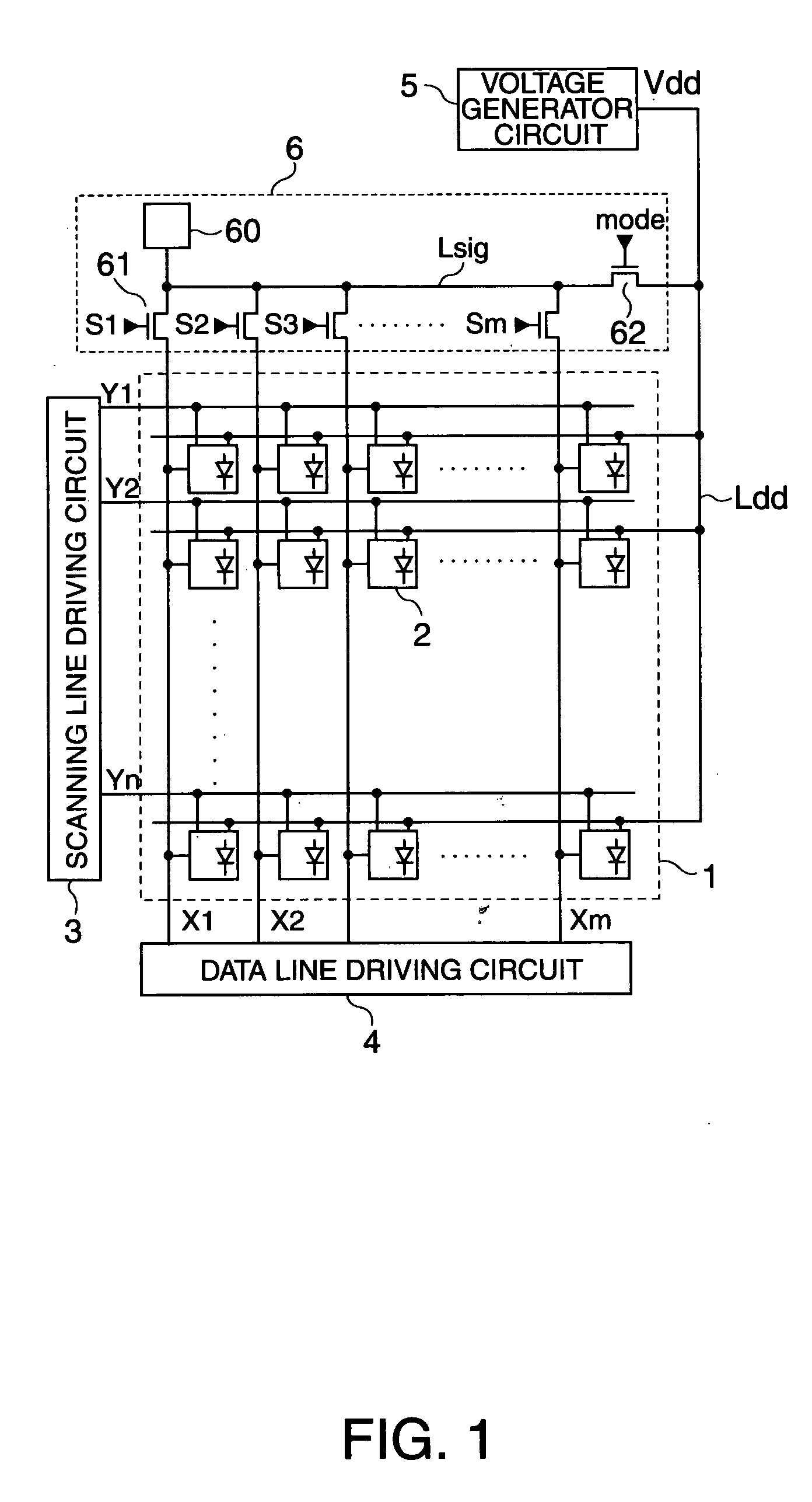
[0026]FIG. 1 is a block schematic of an electro-optical device of a first exemplary embodiment of the present invention. Arranged on a display 1 are a matrix of pixels 2 of n rows by m columns (in a two-dimensional plane), a group of scanning lines Y1-Yn extending in a horizontal direction, and a group of data lines X1-Xm extending in a vertical direction. The pixels 2 are arranged at intersections of the group of scanning lines Y1-Yn and the group of data lines X1-Xm. Power source lines Ldd are supplied with a power source voltage Vdd generated in a voltage generator circuit 5. Each pixel 2 is powered through the power source line Ldd. FIG. 1 does not show a power source line to supply each pixel 2 with a reference voltage Vss lower in level than the power source voltage Vdd, and a driving signal line to supply the pixels with a driving signal GP, to be discussed later, on a row by row basis.

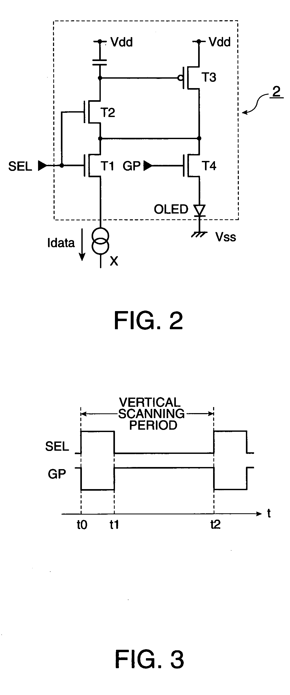
[0027]FIG. 2 is a circuit schematic of one example of pixel 2. A single pixel 2 includes a...

second exemplary embodiment

[0044]FIG. 5 is a circuit schematic illustrating the data write operation for writing data to the pixel 2 in accordance with a second exemplary embodiment of the present invention. In FIG. 5, circuit elements already discussed with reference to FIG. 4 are designated with the same reference numerals, and the discussion thereof is omitted here. The feature of the second exemplary embodiment is that a transistor 63 configured in a diode-mode connection is added in the test circuit 6. The transistor 63 is arranged along the signal transfer line Lsig between the first switching element 61 and the second switching element 62, and has the same characteristics as those of the transistor T3 functioning as a programming transistor. As the data line X is supplied with a voltage lower than the power source voltage Vdd by a threshold voltage Vth of the transistor T3, the signal transfer line Lsig is supplied with a voltage lower than the power source voltage Vdd by a threshold voltage Vth of the...

third exemplary embodiment

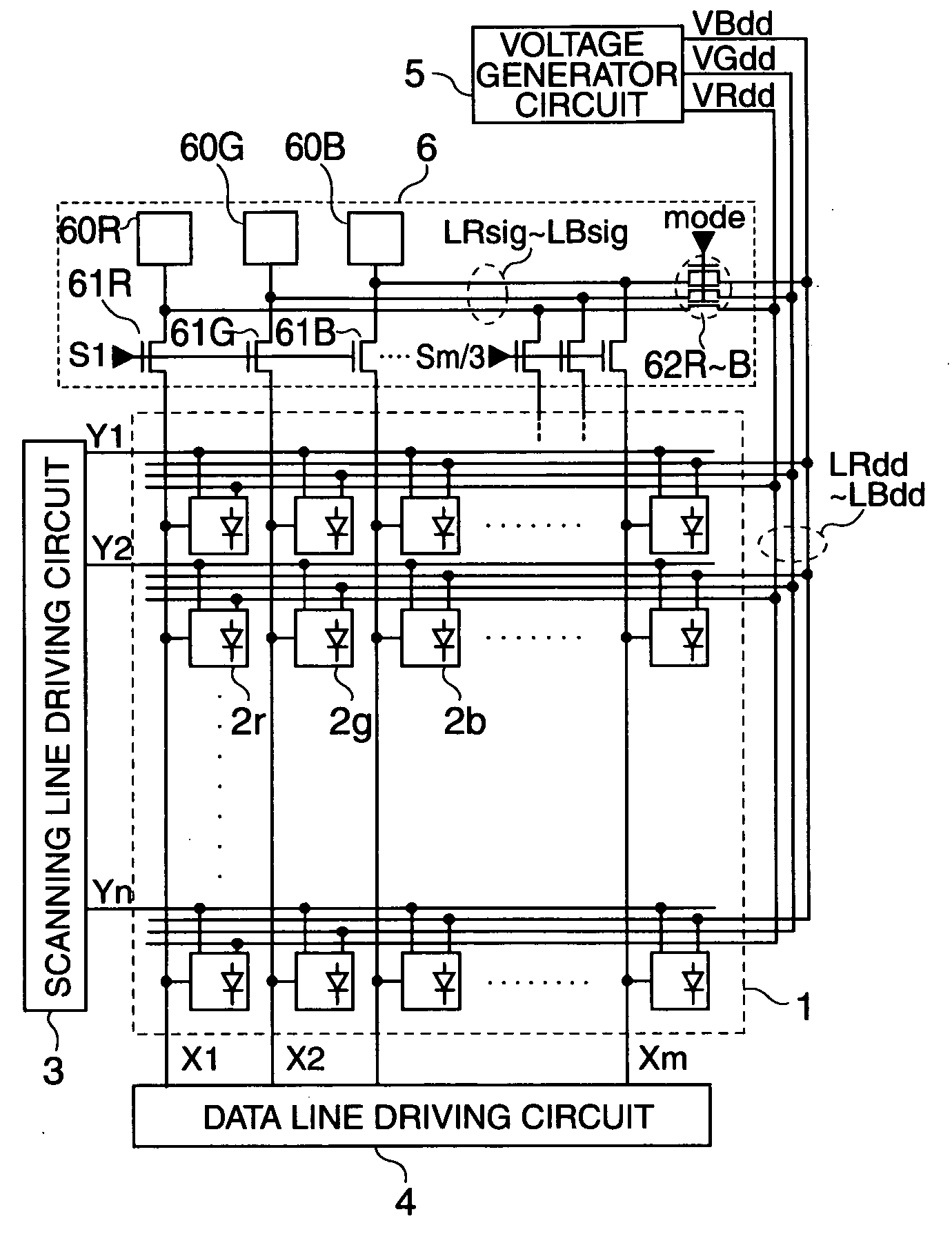
[0045] In accordance with a third exemplary embodiment, voltages of the signal transfer lines Lsig are independently set for R (red), G (green), and B (blue). FIG. 6 is a schematic illustrating an electro-optical device of the third exemplary embodiment of the present invention. One pixel, which is a minimum element of an image, is composed of an R pixel 2r connected to a power source line LRdd for the R, a G pixel 2g connected to a power source line LGdd for the G, and a B pixel 2b connected to a power source line LBdd for the B. The three lines of the power source line LRdd, the power source line LGdd and the power source line LBdd are arranged to set the power source voltages Vdd for respective RGB colors taking into consideration that the organic electro-luminescent elements OLED are different in optical characteristics from R to G to B. The voltage generator circuit 5 generates separately a driving voltage VRdd for the R, a driving voltage VGdd for the G, and a driving voltage ...


PUM


Abstract

To suppress an off leak current of a switching element arranged along a data line to control degradation of tonal gradation in an arrangement in which an organic electro-luminescent element OLED is driven using a current programming method, a first switching element is set to be in a non-conductive state and a second switching element is set to be in a conductive state during a normal mode. During a test mode, the first switching element is set to be in a conductive state while the second switching element is set to be in a non-conductive state.

Description

BACKGROUND OF THE INVENTION [0001] 1. Field of Invention [0002] The present invention relates to an electro-optical device, a method to drive the electro-optical device, and an electronic apparatus and, in particular, to a leak prevention remedy to reduce or prevent a leakage of a current-based data signal supplied to a data line. [0003] 2. Description of Related Art [0004] Displays using organic EL (Electronic Luminescence) element are popular. The organic EL element is a typical current-driven type element that is driven by a current flowing therethrough, and emits luminance in response to a current level. As one of related art driving methods of organic EL elements, a current program method to supply data to a data line in the form of a current is disclosed in Japanese Unexamined Patent Application Publication No. 2003-22049 and Japanese Unexamined Patent Application Publication No. 2003-22050. The current program method has the advantage that variations in TFT (Thin Film Transis...

Claims


Application Information

Patent Timeline
Patent Type & Authority Applications(United States)
IPC IPC(8): H05B33/12G09G3/00G09G3/20G09G3/30G09G3/32H01L51/50
CPCG09G3/006G09G3/3283G09G2300/0842G09G2330/12G09G2310/0262G09G2320/02G09G2330/028G09G2300/0861F16B35/041F16L3/1016
Inventor NAKANISHI, HAYATOOZAWA, TOKUROMIYAZAWA, TAKASHI
Owner ELEMENT CAPITAL COMMERCIAL CO PTE LTD
Why Eureka
Try Eureka