

Semiconductor device and method for fabricating the same
a technology of semiconductors and semiconductors, applied in the direction of semiconductor devices, electrical equipment, transistors, etc., can solve the problems of gate electrode depletion, reduced saturation current value due to depletion, and difficult to avoid both
- Summary
- Abstract
- Description
- Claims
- Application Information
AI Technical Summary
Benefits of technology
Problems solved by technology
Method used
Image

Examples
first embodiment
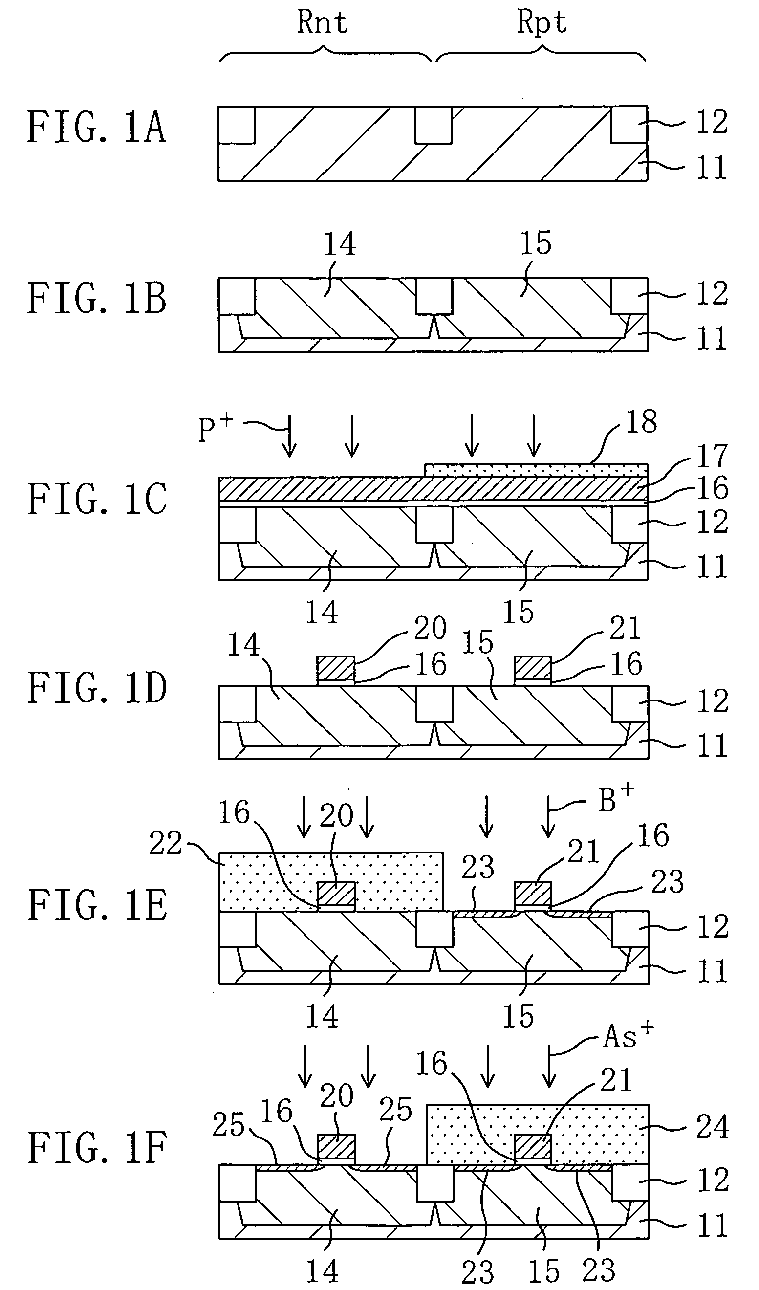
[0037] (First Embodiment)
[0038]FIGS. 1A through 1F and FIGS. 2A through 2E are cross-sectional views illustrating respective steps for fabricating a semiconductor device according to a first embodiment of the present invention. In this embodiment, respective process steps for fabricating a semiconductor device having a single-layer polysilicon gate structure and a dual gate structure will be described.
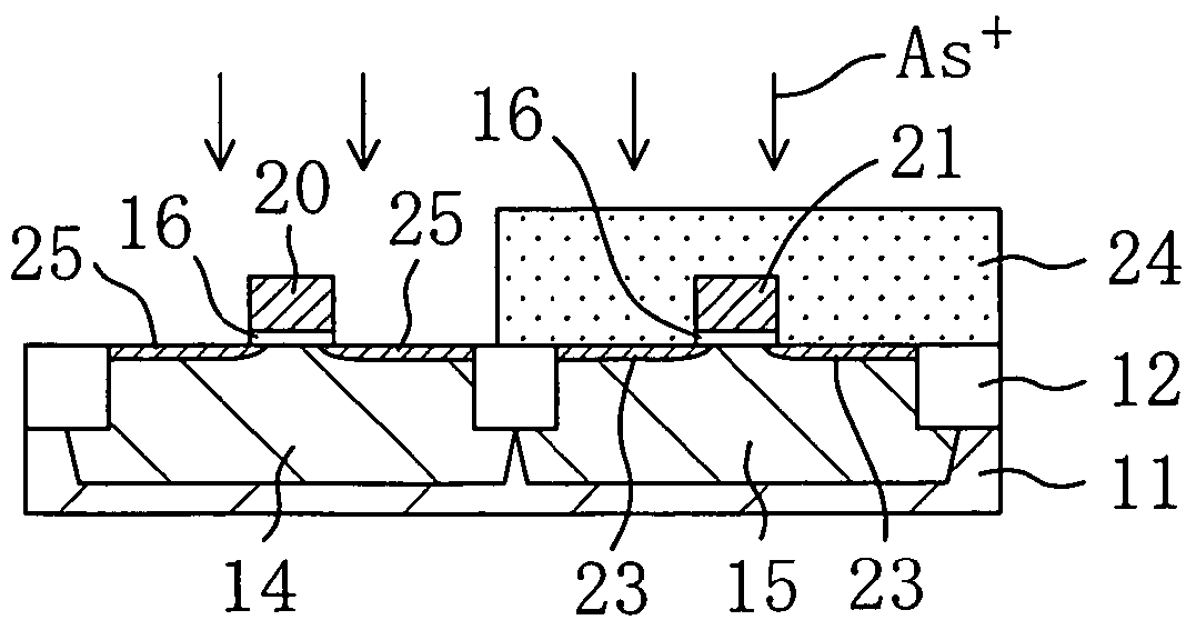
[0039] First, in the process step of FIG. 1A, an isolation region 12 for dividing a surface region into a plurality of active regions is formed on a p-type semiconductor substrate (silicon substrate) 11, and then, in the process step of FIG. 1B, impurity injection for adjusting threshold and impurity injection for forming a well are performed to form a p-type well 14, i.e., an active region for an n-channel MISFET (NMISFET formation region Rnt) and an n-type well 15, i.e., an active region for a p-channel MISFET (PMISFET formation region Rpt).
[0040] Next, in the process step of FIG. ...
second embodiment
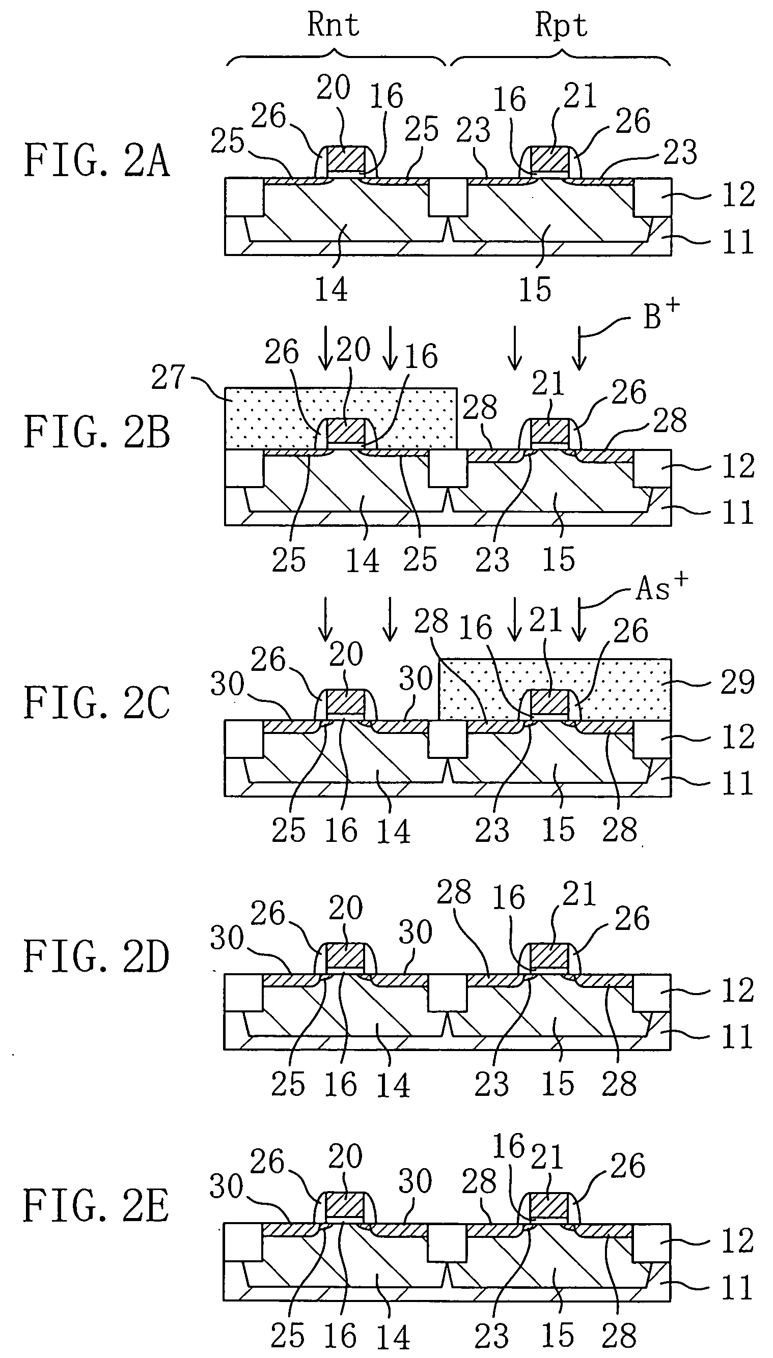
[0058] (Second Embodiment)
[0059]FIGS. 3A through 3F and FIGS. 4A through 4E are cross-sectional views illustrating respective steps for fabricating a semiconductor device of a second embodiment of the present invention. In this embodiment, respective steps for fabricating a semiconductor device having a two-layer polysilicon gate structure and a dual gate structure will be described.
[0060] First, in the process step of FIG. 3A, an isolation region 12 for dividing a surface region into a plurality of active regions is formed on a p-type semiconductor substrate 11 (silicon substrate), and then, in the process step of FIG. 3B, impurity injection for adjusting threshold and impurity injection for forming a well are performed to form a p-type well 14, i.e., an active region for an n-channel MISFET (NMISFET formation region Rnt) and an n-type well 15, i.e., an active region for a p-channel MISFET (PMISFET formation region Rpt).
[0061] Next, in the process step of FIG. 3C, a gate insulati...
third embodiment
[0082] (Third Embodiment)
[0083]FIG. 6 is a cross-sectional view illustrating a semiconductor device according to a third embodiment of the present invention. In this embodiment, a semiconductor device having a two-layer polysilicon gate structure and a dual gate structure will be described. A method for fabricating a semiconductor device according to this embodiment is basically the same as that of the second embodiment. Therefore, illustration and description will be omitted.
[0084] As shown in FIG. 6, the semiconductor device of this embodiment includes an NMISFET and a PMISFET each of which is provided in an active region surrounded by the isolation region 12. The NMISFET includes a p-type well 14 formed in part of a semiconductor substrate 11, a gate insulating film 16 formed on the p-type well 14, a gate electrode 20 formed on the gate insulating film 16, a sidewall 26 covering a side surface of the gate electrode 20, a source / drain region including a lightly doped impurity reg...
PUM
| Property | Measurement | Unit |
|---|---|---|
| temperature | aaaaa | aaaaa |
| temperature | aaaaa | aaaaa |
| temperature | aaaaa | aaaaa |
Abstract
Description
Claims
Application Information