

Polymer-based memory element
a polymer and memory element technology, applied in thermoelectric devices, instruments, nanoinformatics, etc., can solve the problems of increasing reducing the efficiency of traditional solid-state memory devices, and increasing the cost of vaporization of memory elements, so as to increase or decrease the resistance of organic polymers.
- Summary
- Abstract
- Description
- Claims
- Application Information
AI Technical Summary
Benefits of technology
Problems solved by technology
Method used
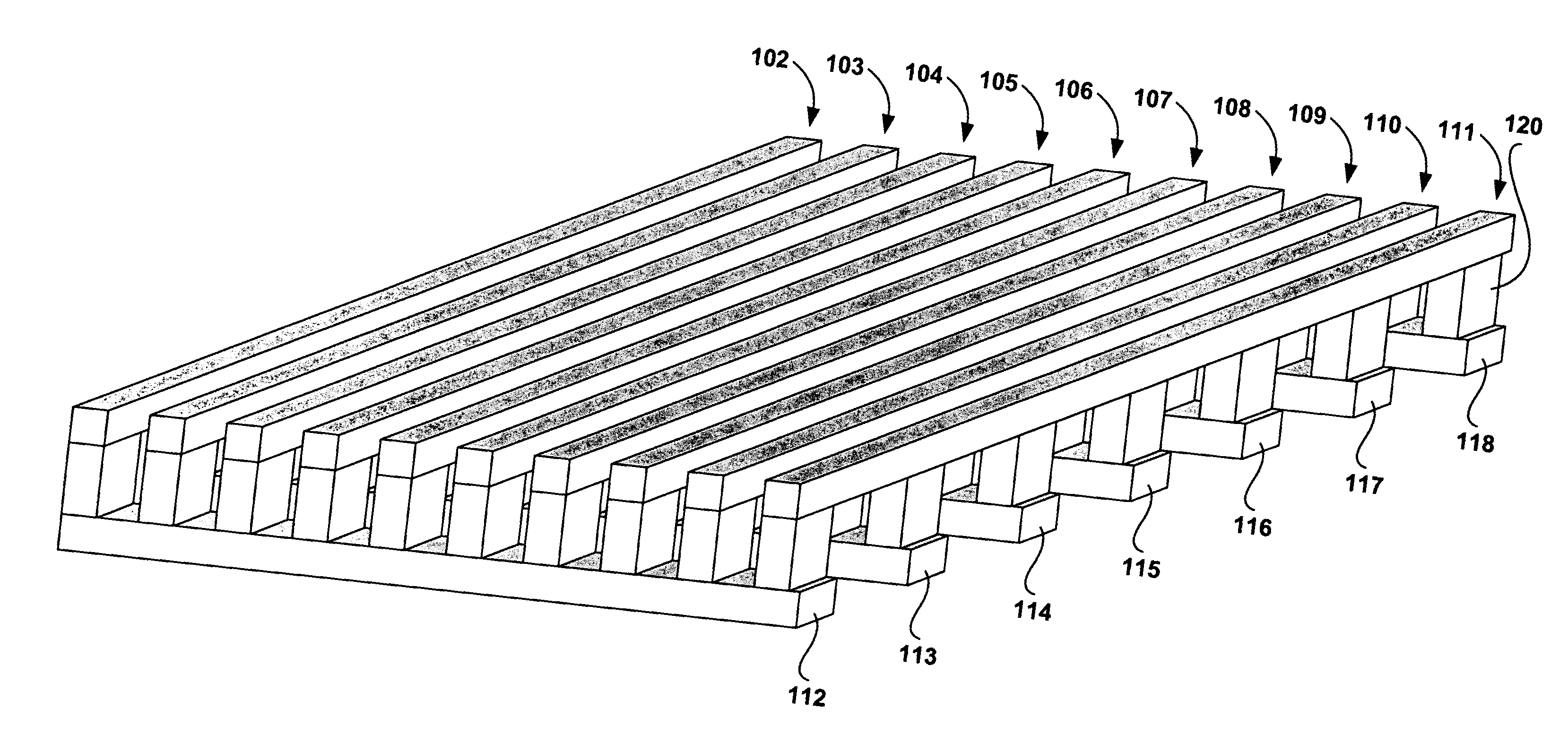
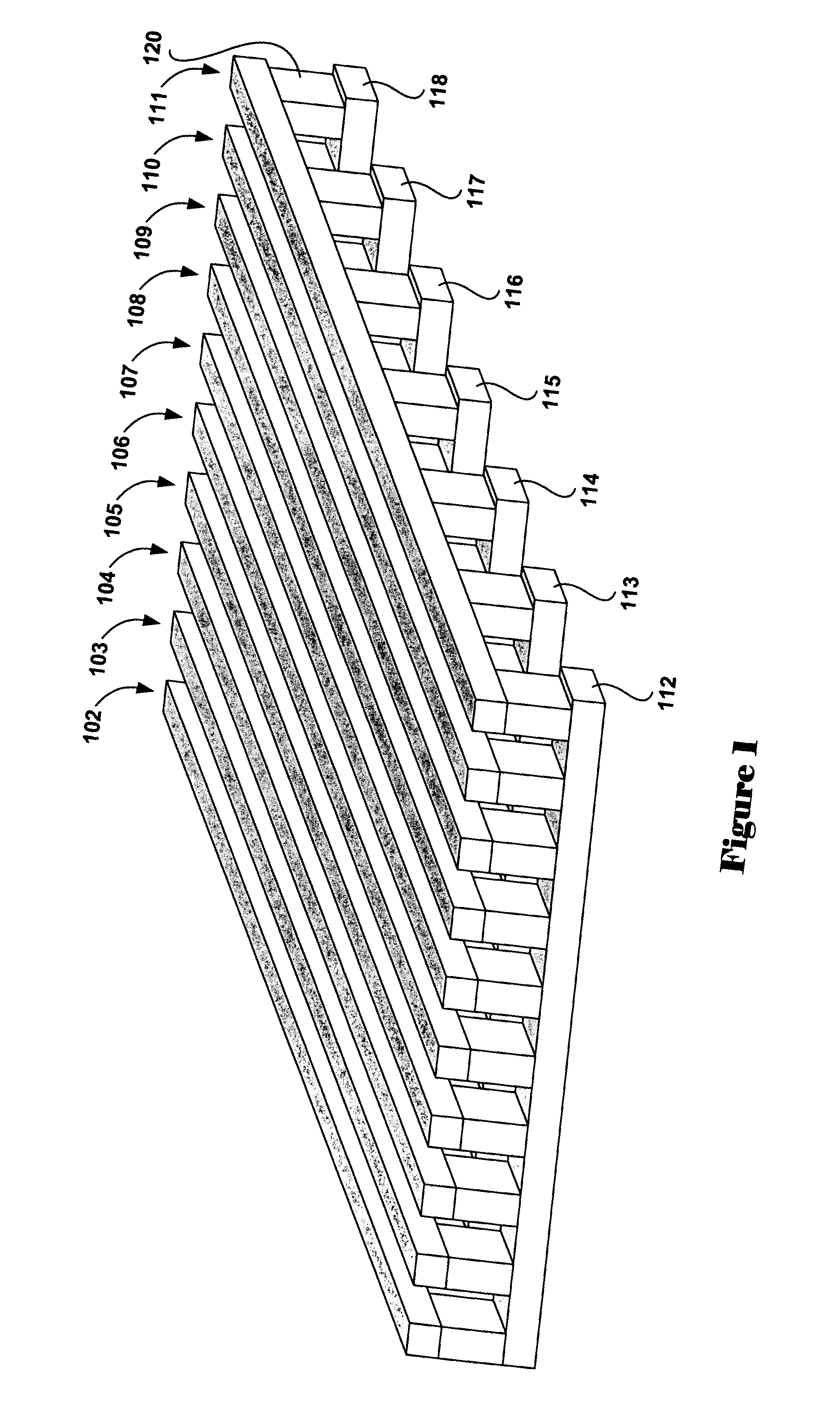
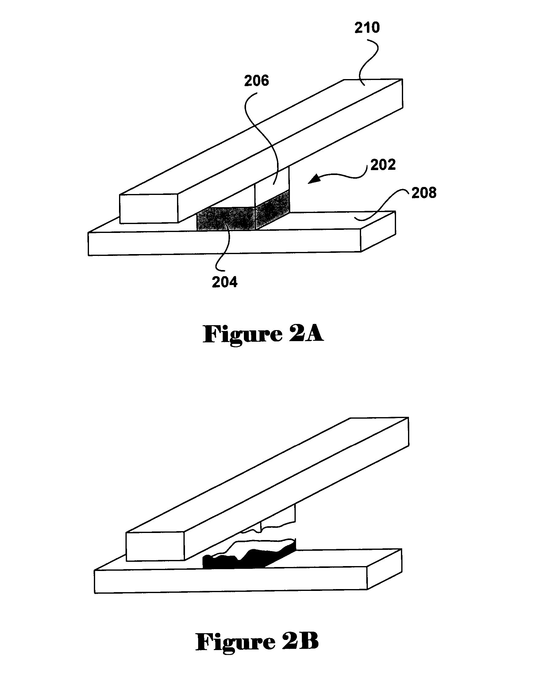
Image

Examples
Embodiment Construction
[0019] Most synthetic and naturally occurring organic polymers are insulators. During the past 30 years, large research efforts have been devoted to developing conductive organic polymers for use in a wide variety of different electrical applications. Currently, a rather large number of highly conductive organic polymers are known, and the research efforts undertaken to identify and synthesize conductive polymers have provided great insight into the nature of conductive organic polymers. FIGS. 3A-C illustrate a conductive organic polymer. FIG. 3A shows a chemical notational representation of the conductive organic polymer polyphenylenevinylene. The polyphenylenevinylene polymer is a long chain of repeating phenylenevinylene monomer subunits. A segment of the chain is shown in FIG. 3A. Polymer chains may extend for tens to hundreds to even thousands of monomer subunits. Naturally occurring biopolymers, such as DNA, may extend to millions of covalently linked subunits. The polyphenyle...
PUM
| Property | Measurement | Unit |
|---|---|---|
| Electronic properties | aaaaa | aaaaa |
| Electrical resistance | aaaaa | aaaaa |
| Electrical conductance | aaaaa | aaaaa |
Abstract
Description
Claims
Application Information