Columnar floorplan

a floor plan and column technology, applied in the field of integrated circuits, can solve the problems of increasing the cost of an integrated circuit die directly related to its size, increasing the cost of an integrated circuit die to produce, and the layout of an integrated circuit die includes considerable engineering effort and therefore cost. , to achieve the effect of reducing the cost of the integrated circui

Inactive Publication Date: 2005-01-13
XILINX INC
View PDF21 Cites 50 Cited by
  • Summary
  • Abstract
  • Description
  • Claims
  • Application Information

AI Technical Summary

Benefits of technology

[0020] The circuitry of an FPGA is laid out as a plurality of repeatable tiles. The word “tile” used herein means an area comprising circuitry with one or more programmable functions, including memory, or dedicated circuitry. A tile may, although not necessarily, include programmable interconnections such as a CLB tile. The tiles are disposed in columns. Each column extends all the way across the die from one side of the die (for example, the top side) to an opposite side of the die (for example, the bottom side). Each column consists essentially of tiles of only one type. Rather than providing a ring of input/output blocks (IOBs) around the periphery of the die that would break the columnar tile structure of the layout, the IOB tiles of the FPGA are disposed in columns only.

Problems solved by technology

The cost of an integrated circuit die is directly related to its size.
If all other cost factors involved in the manufacture of an integrated circuit are equal, then making the integrated circuit larger will make the integrated circuit more expensive to produce.
Because the layout of an integrated circuit die includes considerable engineering effort and therefore cost, FPGA integrated circuits are often laid out as a set of repeatable “tiles”.
This additional capacitive loading is undesirable.
In addition to an undesirable increase in capacitive loading, providing both a bond bump and a wire bond pad also has the drawback of consuming additional die surface area.
Wire bond pads cannot generally be disposed directly over areas of circuitry.
The physical forces imposed on the wire bond pad may damage any circuitry that might be disposed under the wire bond pad.
Accordingly, the IOI tile mechanism for interfacing IOB tiles to the central core cannot easily be used in the four corner areas of the die.
In addition to the limited utility of corner regions 12-15, the tiles and layout technique of FIG. 1 also results in areas above and below the columns of BRAM/multiplier tiles having limited utility.
A clock management circuit may, for example, occupy a smaller area than is available in one of these areas such that some

Method used


Image

  • Columnar floorplan
  • Columnar floorplan
  • Columnar floorplan

Examples


Embodiment Construction

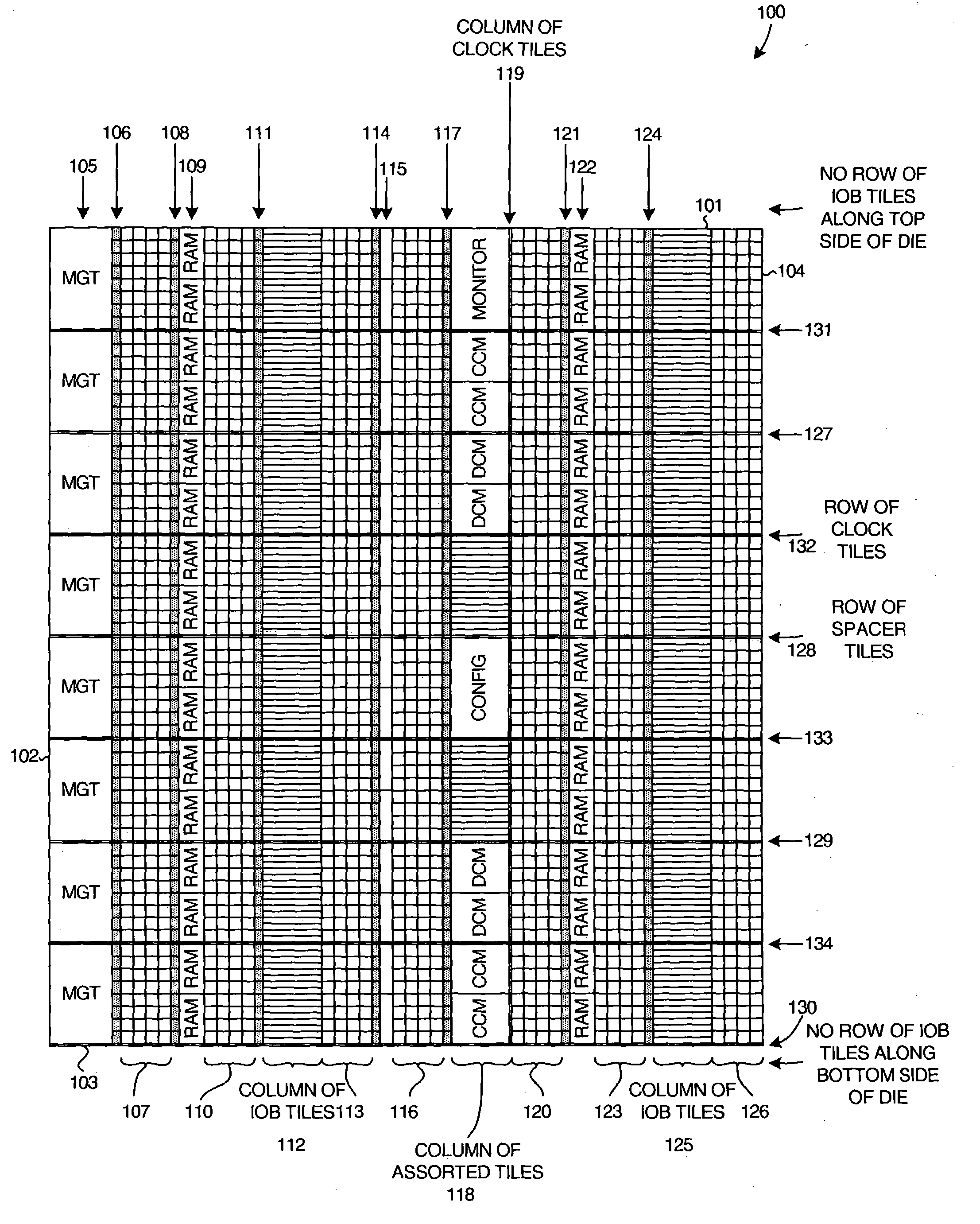
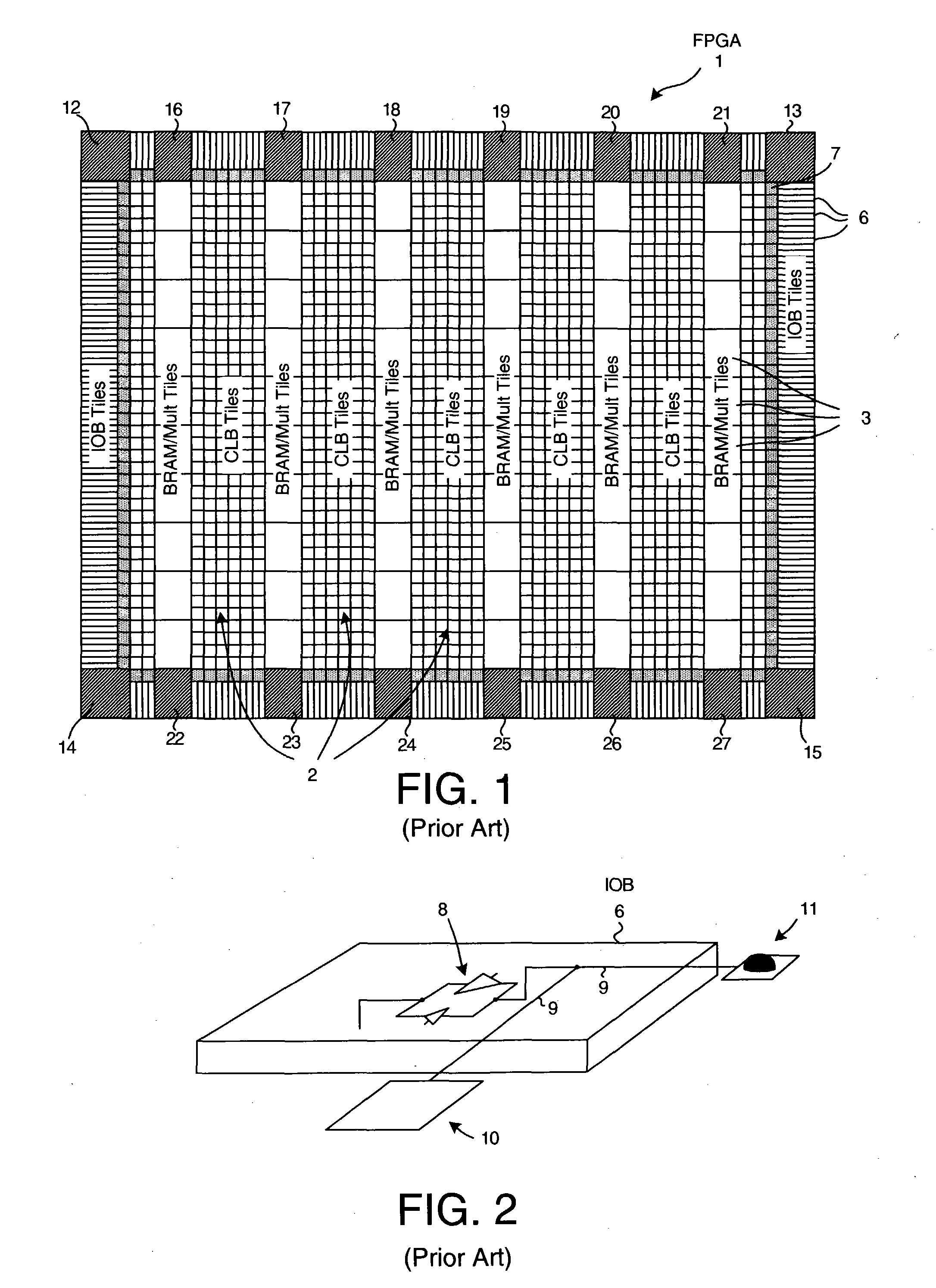
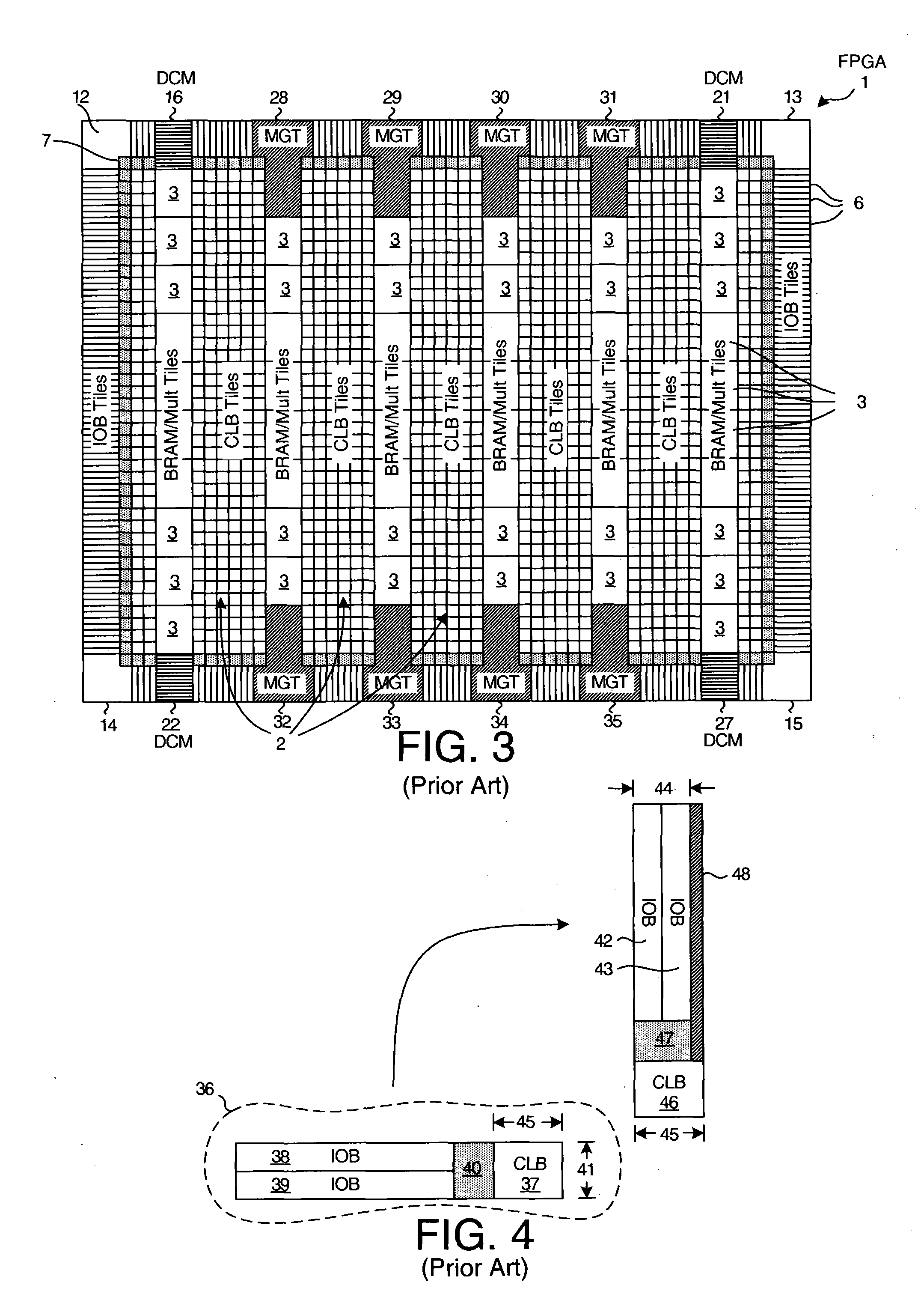
[0035]FIG. 5 is a simplified top-down diagram of a field programmable gate array (FPGA) integrated circuit die 100 in accordance with an embodiment of the present invention. FPGA die 100 is rectangular and has four sides 101-104. The circuitry of the FPGA is laid out across the surface of die 100 as a plurality of columns of repeatable tiles. Proceeding from the left side 102 of die 100 to the right side 104 of die 100, there is a column of identical multi-gigabit transceiver (MGT) tiles 105, a column of input / output interconnect (IOI) tiles 106, four columns of configurable logic block (CLB) tiles 107, a column of IOI tiles 108, a column of block random access memory (BRAM) tiles 109, four columns of CLB tiles 110, a column of IOI tiles 111, a column of input / output block (IOB) tiles 112, four columns of CLB tiles 113, a column of IOI tiles 114, a column of digital signal processing (DSP) tiles 115, four columns of CLB tiles 116, a column of IOI tiles 117, an irregular column 118 m...


PUM


Abstract

An FPGA is laid out as a plurality of repeatable tiles, wherein the tiles are disposed in columns that extend from one side of the die to another side of the die, and wherein each column includes tiles primarily of one type. Because substantially all die area of a column is due to tiles of a single type, the width of the tiles of each column can be optimized and is largely independent of the size of the other types of tiles on the die. The confines of each type of tile can therefore be set to match the size of the circuitry of the tile. Rather than providing a ring of input/output blocks (IOBs) around the die periphery, IOB tiles are disposed in columns only. Where more than two columns worth of IOBs is required, more than two columns of IOB tiles can be provided.

Description

FIELD OF THE INVENTION [0001] The present invention relates to integrated circuits that are laid out in tiles. BACKGROUND INFORMATION [0002] Programmable logic devices (PLDs), such as field-programmable gate arrays (FPGAs), are user-programmable integrated circuits that can be programmed to implement user-defined logic circuits. In a typical FPGA architecture, an array of configurable logic blocks (CLBs) and a programmable interconnect structure are surrounded by a ring of programmable input / output blocks (IOBs). Configurable logic blocks can also be referred to using other names such as, for example, a logic array block (LAB) or a logic module. [0003] In one SRAM-based FPGA, each of the CLBs, each of the IOBs, and the programmable interconnect structure includes configuration memory cells, the contents of which determine how the CLB, the programmable interconnect structure, or the IOB is configured. To realize a user-defined circuit, configuration data is loaded into the configurat...

Claims


Application Information

Patent Timeline
IPC IPC(8): G06F17/50H01L27/02H01L27/118H03K19/177
CPCH01L27/0207H01L27/11898H01L27/11807H01L27/11803
Inventor YOUNG, STEVEN P.
Owner XILINX INC
Why Eureka
Try Eureka