Defect inspection of extreme ultraviolet lithography masks and the like

Active Publication Date: 2005-01-13
WISCONSIN ALUMNI RES FOUND
View PDF6 Cites 36 Cited by
  • Summary
  • Abstract
  • Description
  • Claims
  • Application Information

AI Technical Summary

Benefits of technology

[0010] The present invention provides a method for defect inspection of extreme ultraviolet (EUV) lithography masks and the like. A method in accordance with the present invention may be used to find defects in EUV mask blanks with both high sensitivity, i.e., the ability to detect very small defects, and accuracy, i.e., the ability to reject backg

Problems solved by technology

By such a dark field method, only defects appear in the field of view of the inspection system.
If, however, the blank has defects, the area immediately above and surrounding a defect on the mask blank surface will receiv

Method used


Image

  • Defect inspection of extreme ultraviolet lithography masks and the like
  • Defect inspection of extreme ultraviolet lithography masks and the like
  • Defect inspection of extreme ultraviolet lithography masks and the like

Examples


Example

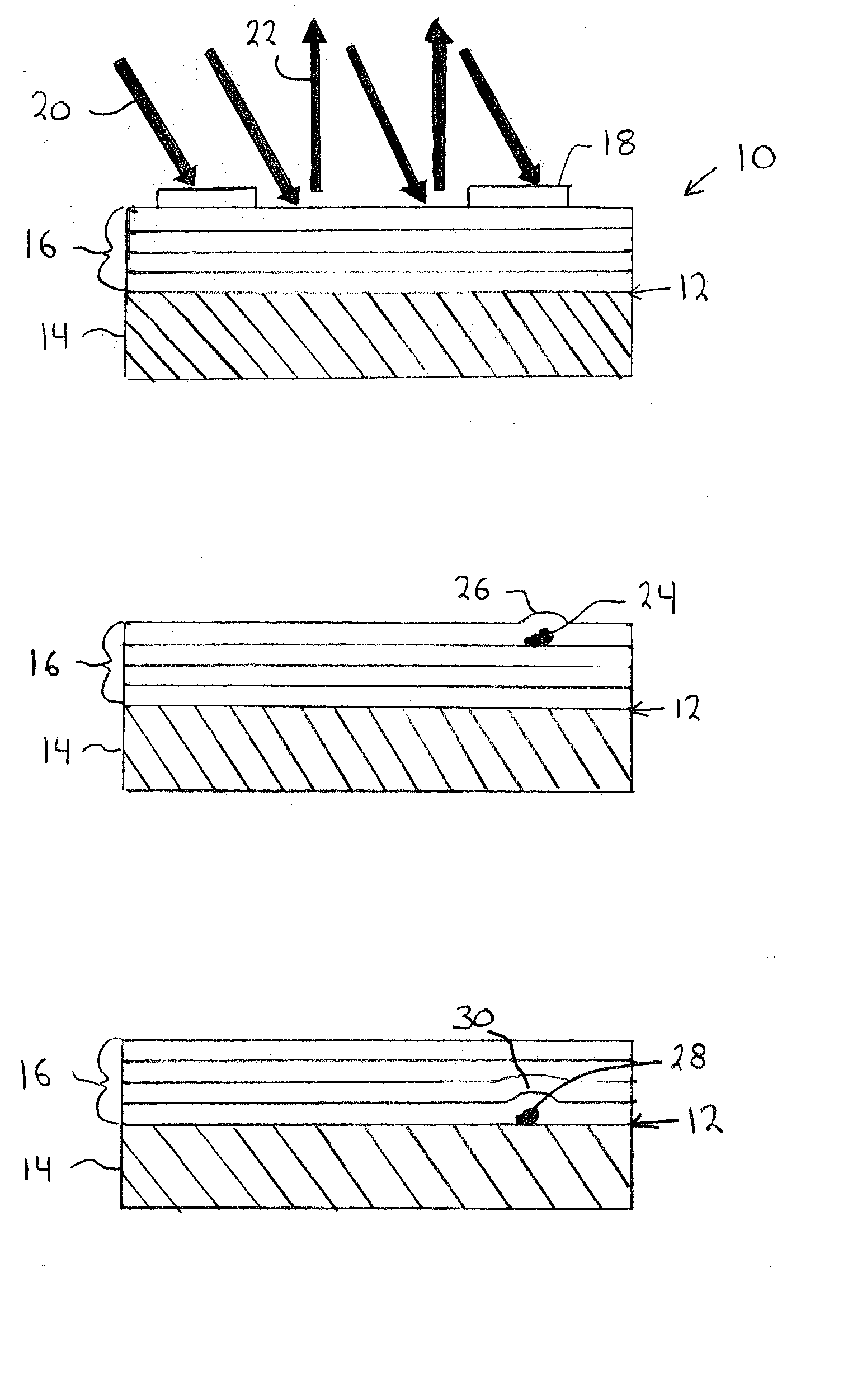
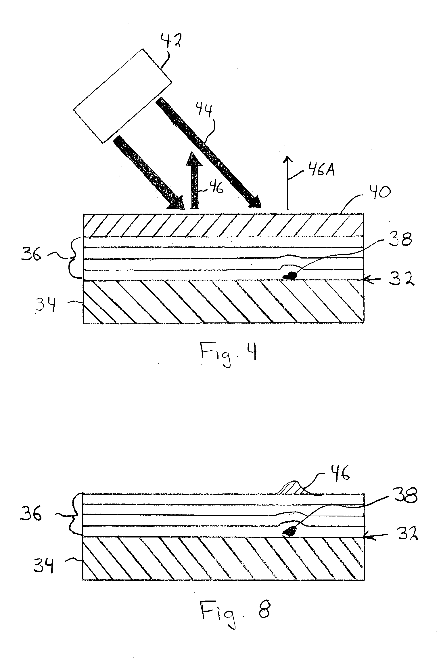
[0023] A method for the detection of defects in extreme ultraviolet (EUV) lithography masks and the like in accordance with the present invention now will be described in detail beginning with reference to FIG. 4. FIG. 4 is a schematic cross-sectional illustration of a lithography mask blank 32 (e.g., an EUV lithography mask blank) to be inspected for defects in accordance with the present invention. As discussed above, the EUV mask blank 32 may include a reflective substrate 34 upon which is formed an interference stack 36, which enhances the reflectivity of the mask blank 32. One or more defects 38 may, or may not, be present in the mask blank. As is discussed above, a defect 38 in the mask blank, e.g., on or near the surface of the substrate 34 or in the interference stack 36, may destroy the effectiveness of a lithography mask formed from the mask blank 32. Specifically, the defect 38 in the mask blank will cause a phase shift in the EUV or other radiation reflected from the mas...


PUM


Abstract

A dark-field imaging method for detecting defects in reflective lithography masks (e.g., extreme ultraviolet (EUV) masks) used, e.g., in processes for the fabrication of microelectronic devices. A mask blank is coated with a photoresist layer having a fluorescent dye incorporated therein. The photoresist layer is exposed to a source of radiation (e.g., EUV radiation or glancing soft X-rays). In areas of the mask blank having defects the combined direct and reflected radiation will be insufficient fully to expose the photoresist layer. After development, photoresist will remain on the mask blank surface in areas corresponding to defects. Illumination with the excitation wavelength of the fluorescent dye reveals the location of any remaining photoresist, which can be detected using an optical microscope, thereby to detect defects in the mask blank.

Description

FIELD OF THE INVENTION [0001] This invention pertains generally to masks used in lithography processes for the fabrication of microelectronic devices and micromechanical structures, and more particularly to masks used in extreme ultraviolet (EUV) lithography and methods and devices for inspecting such masks to determine if there are defects therein. BACKGROUND OF THE INVENTION [0002] Lithography is at the heart of processes for the fabrication of microelectronic devices, such as integrated circuits, and micromechanical structures. The basic process of producing a microelectronic device involves the modification of the surface material of a semiconductor substrate, such as of silicon, in a pattern. The interplay of the material changes and the pattern defines the electrical characteristics of the microelectronic device. A similar process can be used to form micromechanical devices, by, for example, electroplating metal structures in a desired pattern onto a substrate. Lithography is ...

Claims


Application Information

Patent Timeline
IPC IPC(8): G01N21/84G01N21/956G03F1/00G03F1/14G03F9/00G03G16/00G06K9/00G06T7/00G21K5/00
CPCB82Y10/00B82Y40/00G01N21/8422G03F1/24Y10S430/168G06T7/0004G06T2207/30148Y10S430/143Y10S430/167G03F1/84
Inventor CERRINA, FRANCESCOPAWLOSKI, ADAMWANG, LIN
Owner WISCONSIN ALUMNI RES FOUND
Why Eureka
Try Eureka