Method and apparatus for manufacturing image displaying apparatus

a technology of image displaying apparatus and manufacturing method, which is applied in the manufacture of electrode systems, electric discharge tubes/lamps, and tube/lamp factory adjustment. it can solve the problems of vacuum exhausting of each vacuum chamber, inconvenient, and long time, and achieve excellent electron emission characteristics, reduce vacuum exhaust time, and high vacuum degree

Inactive Publication Date: 2005-01-13
CANON KK
View PDF34 Cites 14 Cited by
  • Summary
  • Abstract
  • Description
  • Claims
  • Application Information

AI Technical Summary

Benefits of technology

The present invention has an object to manufacture an electron source having an excellent electron-emitting characteristic, and to easily attain a reduction of vacuum exhaust time and a high vacuum degree, thereby improving a manufacturing efficiency.
Further, the present invention has another object to provide a method and a manufacturing apparatus of an electron source substrate and an image displaying apparatus which can easily be reduced in size and simplified in its operation.

Problems solved by technology

The manufacturing method according to the conventional art described above requires considerably long time for manufacturing one display panel, thus is not suitable for manufacturing a display panel inside of which requires the vacuum degree of 10−6 Pa or more.
Also, the second manufacturing method includes a problem in that it takes a long period of time for exhausting a gas from the space within the panels of the image displaying apparatus, and for introducing a gas containing an organic substance into the space with the panel.
In addition, since movement between each vacuum chamber of the FP and the RP is performed with breaking the atmosphere, each vacuum chamber is vacuum exhausted every time an FP and an RP are carried in.
As a result, the manufacturing process time becomes longer.

Method used


Image

  • Method and apparatus for manufacturing image displaying apparatus
  • Method and apparatus for manufacturing image displaying apparatus
  • Method and apparatus for manufacturing image displaying apparatus

Examples


embodiment 1

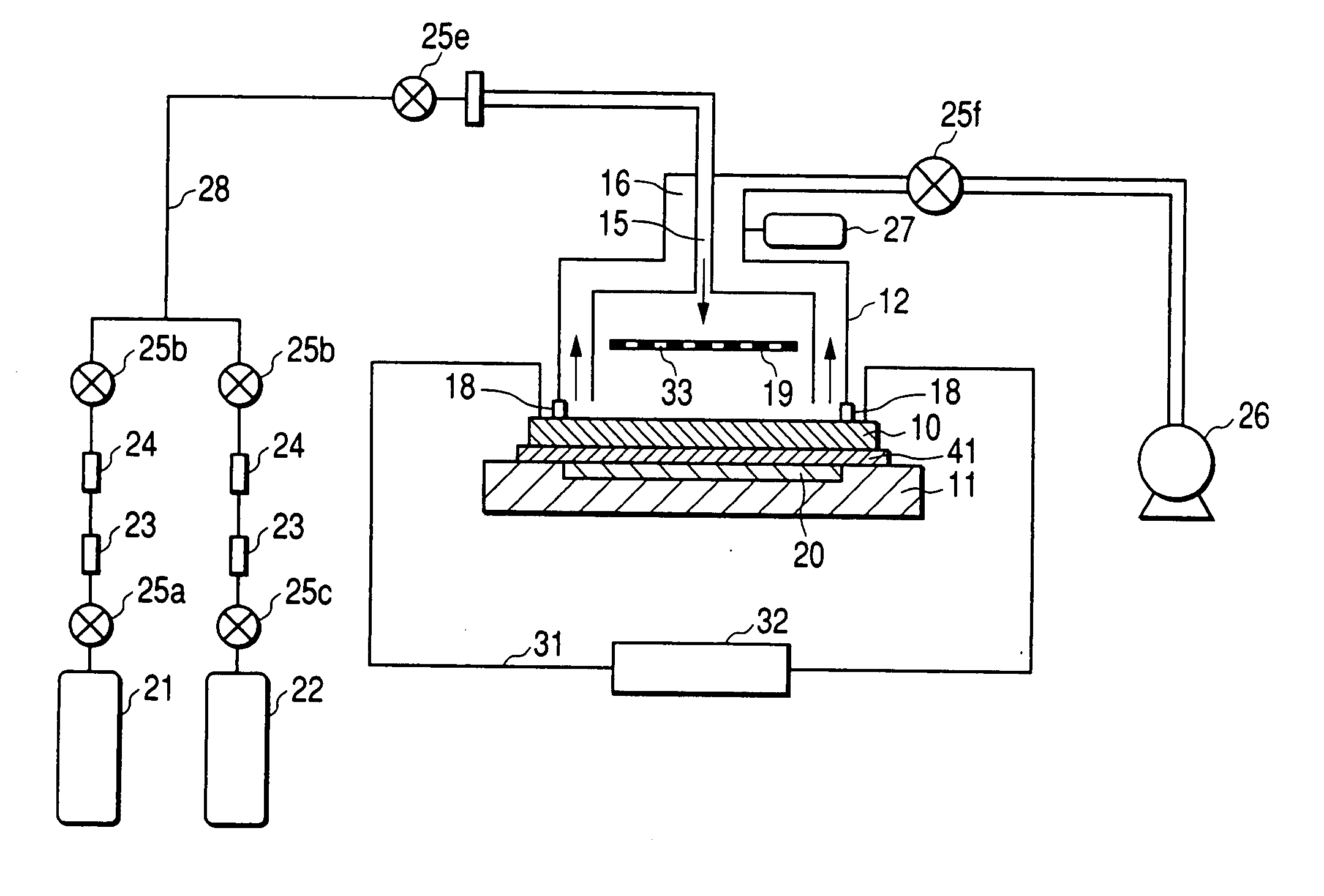
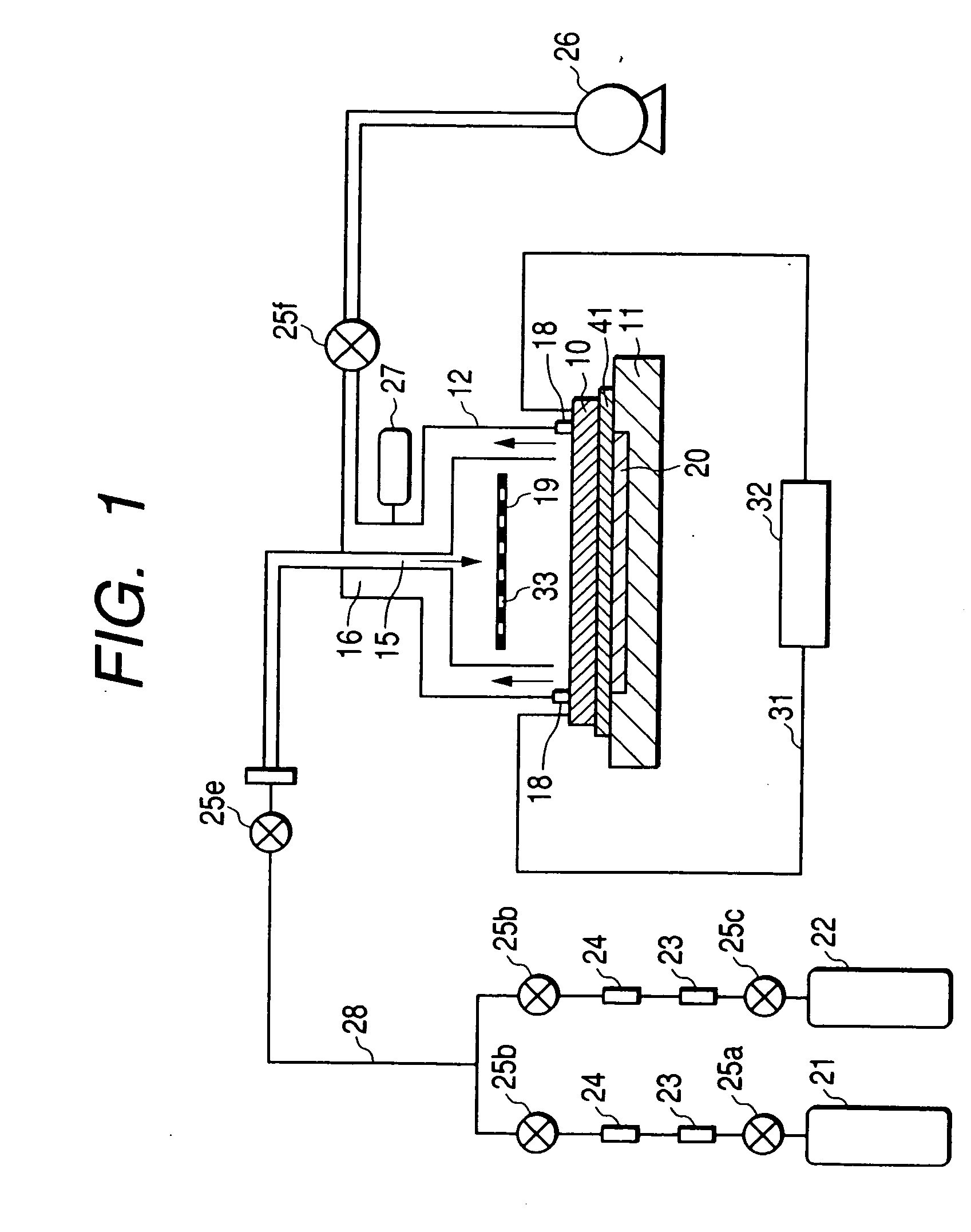
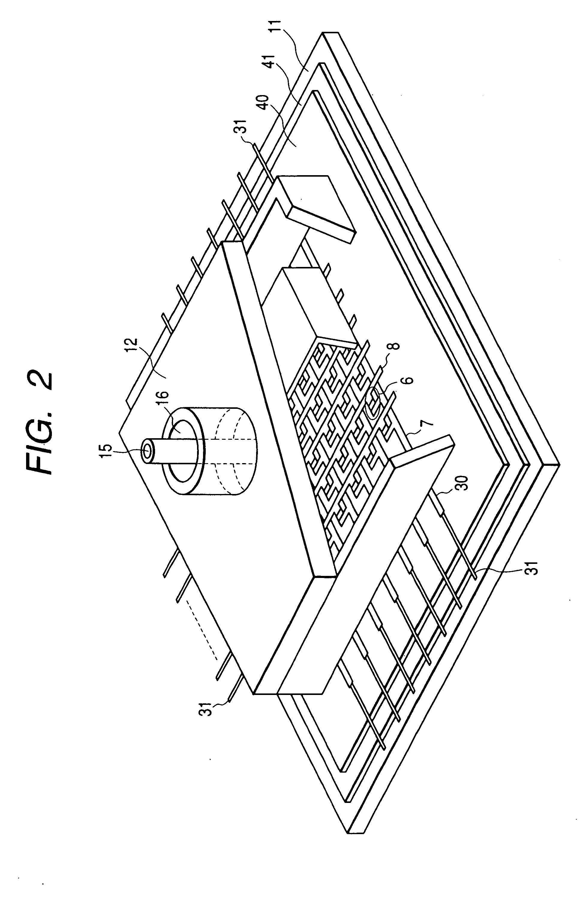
In this embodiment, an electron source shown in FIG. 26 having a plurality of surface conduction electron-emitting devices shown in FIGS. 24 and 25 is formed using the manufacturing apparatus according to the present invention. Note that, in FIGS. 24 and 25, reference numeral 10 is an electron source substrate; 2 and 3, device electrodes; 4, an electroconductive film; 29, a carbon film; 5, a gap of a carbon film 29; and character G is a gap of the electroconductive film 4. On the glass substrate (a size of 350×300 mm, a thickness of 5 mm) forming an SiO2 layer thereon, a Pt paste is printed by an offset printing method, and by subjecting the substrate to heating and baking, the device electrodes 2 and 3 are formed into a thickness of 50 nm as shown in FIG. 27. Besides, by a screen printing method, Ag paste is printed on the substrate, and the heating and baking are carried out to form an X directional wiring 7 (240) and a Y directional wiring 8 (720) as shown in FIG. 27. At the int...

embodiment 2

An electron source substrate 10 shown in FIG. 27 was formed similarly to Embodiment 1, and the electron source substrate 10 was provided in a manufacturing apparatus in FIG. 1. In this embodiment, after heating a mixture gas containing organic substances to 80° C. by a heater provided in the vicinity of a piping 28, the mixture gas was introduced into a vacuum container 12. Besides, the electron source substrate 10 was heated through a thermal conductive member 41 using a heater 20 in a supporting member 11 to set the substrate temperature to 80° C. An activation process was performed as in Embodiment 1 other than the above, to thereby form an electron source.

On the electron-emitting device subjected to the activation process, carbon films 29 are formed with a gap 5 as shown in FIGS. 25 and 26.

In this embodiment as well, the activation process could be performed in a short period of time as in Embodiment 1. When a device current If at the end of the activation process was measu...

embodiment 3

An electron source substrate 10 shown in FIG. 27 was formed similarly to Embodiment 1, and an electron source was formed using the manufacturing apparatus shown in FIG. 3 by the same method as in Embodiment 1 except that silicone oil was used as a thermal conductive member.

In the apparatus according to this embodiment, when silicone oil is injected into the lower portion of the substrate using a pipe for introducing viscous liquid material, a through hole (not shown) that serves for air escape and for discharging the viscous liquid material is provided at a position outside a device electrode region, which is substantially a diagonal line to the pipe. The device current value after the activation process was the same as in Embodiment 1.

Thereafter, using an electron source substrate 10 subjected to the above processes, an image displaying apparatus shown in FIG. 23 is manufactured. First, the electron source substrate 10 and the outer frame 62 are fixed onto the RP 61, and this ...


PUM


Abstract

A method and an apparatus of manufacturing an image displaying apparatus having an electron source substrate and a phosphor substrate. The electron source substrate is provided with an electron emitting element formed by covering with a container and by applying a voltage to an electronic conductor on the substrate. While, the phosphor substrate is provided with a phosphor thereon. The substrates are subjected to a getter processing and to a seal bonding process under a vacuum condition through a processing chamber, to complete an image forming apparatus. An improvement resides in miniaturizing and simplifying operation, and in greater manufacture speed and mass production.

Description

BACKGROUND OF THE INVENTION 1. Field of the Invention The present invention relates to a method of manufacturing an image displaying apparatus in which a plurality of electron sources are arranged, and to an apparatus for manufacturing the same. 2. Related Background Art Conventionally, an electron-emitting device is roughly divided into two known types, i.e., a thermal electron-emitting device and a cold-cathode electron-emitting device. The cold-cathode electron-emitting device includes a field emission type, a metal / insulating layer / metal type, a surface conduction electron-emitting device, and the like. A surface conduction electron-emitting device is to utilize such a phenomenon that electron emission generates by flowing electric current to a thin film with a small area formed on a substrate, in parallel with the surface of the film. The applicant of the present invention made a large number of proposals on the surface conduction electron-emitting device having a novel st...

Claims


Application Information

Patent Timeline
Patent Type & Authority Applications(United States)
IPC IPC(8): H01J1/30H01J9/02H01J9/38
CPCH01J9/027H01J9/38H01J9/385H01J2329/945H01J2201/3165H01J2209/385H01J2329/941H01J31/127H01J1/30
Inventor NOMURA, ICHIRONAKATA, KOHEIKANEKO, TETSUYAMIYAZAKI, TOSHIHIKOSATO, YASUEOHNISHI, TOSHIKAZU
Owner CANON KK
Why Eureka
Try Eureka