

Design-based monitoring
- Summary
- Abstract
- Description
- Claims
- Application Information
AI Technical Summary
Benefits of technology
Problems solved by technology
Method used
Image

Examples
implementation examples
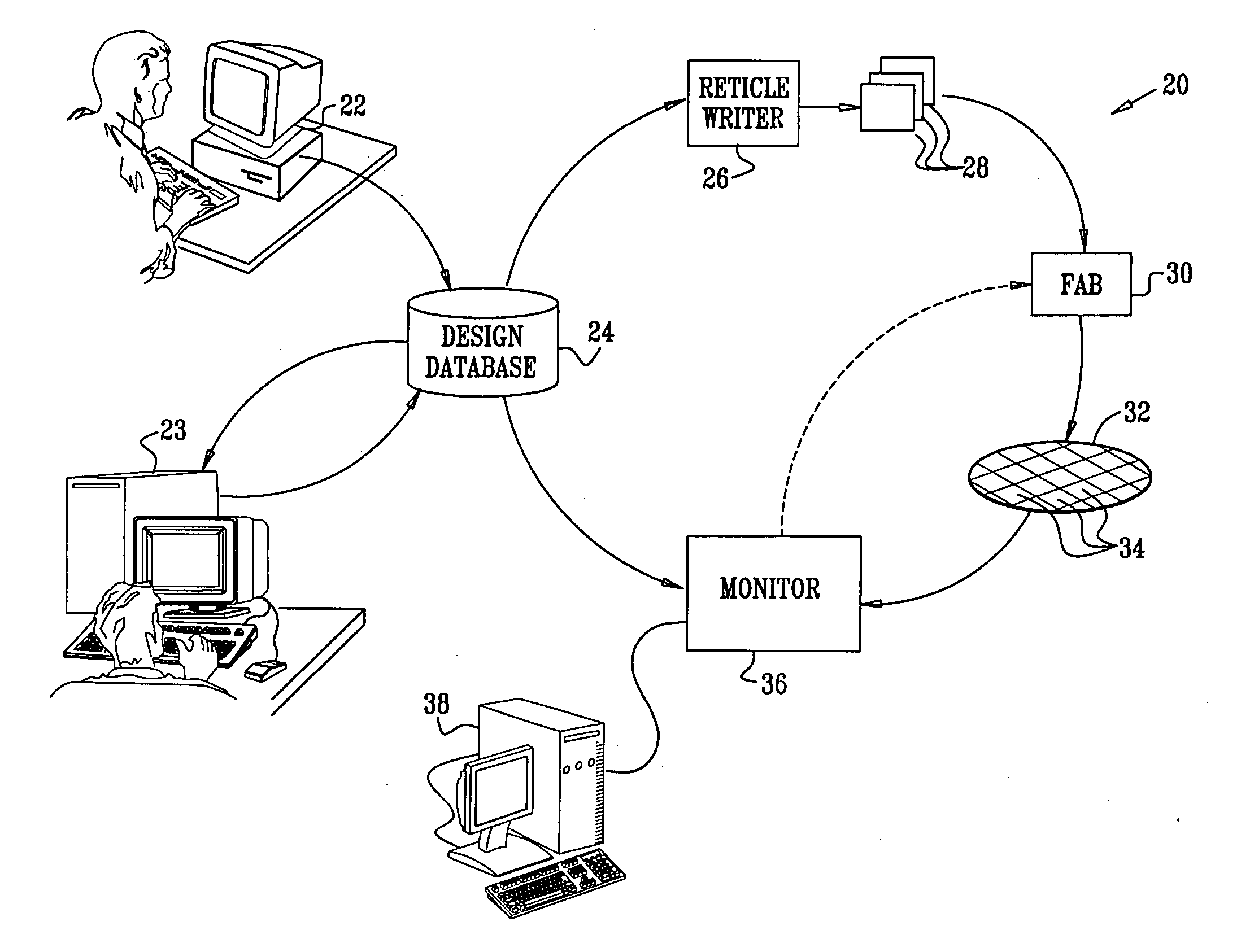
The following section lists a number of exemplary applications of the use of PDP data generated by EDA workstations 22 and 23 (FIG. 1) in driving process monitor 36. These applications may advantageously use the data structures defined above. Alternatively, the relevant PDP data may be conveyed from the EDA tools or database to the appropriate process monitoring tools in other forms and formats.
Selection of Inspection and Measurement Locations
The PDP data may be used in selecting the locations on die 34 that are to be examined in a given monitoring step. This feature of the present invention is useful, for example, in automatic process inspection using e-beam and optical inspection tools, in critical dimension (CD) measurements and in other process monitoring applications. Typically, the locations for monitoring are those that are most susceptible to process faults, and are selected based on sites 56 that have been designated in the design and verification stages. As a result o...
PUM
 Abstract
Description
Claims
Application Information