Magnetic switching element and a magnetic memory

a switching element and magnetic memory technology, applied in the manufacture of flux-sensitive heads, instruments, transistors, etc., can solve the problems of large power consumption of a memory, inability to carry out large-scale memory, and the size cannot be decreased below semiconductor dram, etc., and achieve great merit for the industry

Inactive Publication Date: 2005-01-20
KK TOSHIBA
View PDF6 Cites 10 Cited by
  • Summary
  • Abstract
  • Description
  • Claims
  • Application Information

AI Technical Summary

Benefits of technology

[0067] binary information being recorded as the magnetization in the record layer of the magnetoresistance effect element of a predetermined one of the memory cells by selecting the memory cell and by applying the voltage to either one of the first and second magnetic semiconductor layers.

Problems solved by technology

With regard to the memory cell size, however, those existing techniques involve the problem that the size cannot be decreased below semiconductor DRAM (dynamic random access memory) when a 1 Tr (transistor) −1 TMR architecture (disclosed, for example, in U.S. Pat. No. 5,734,605) is employed.
For this reason, the power consumption of a memory is large, when

Method used


Image

  • Magnetic switching element and a magnetic memory
  • Magnetic switching element and a magnetic memory
  • Magnetic switching element and a magnetic memory

Examples


examples

[0233] Hereafter, some embodiments of the invention will be explained in more detail, referring to a specific example of the invention.

first example

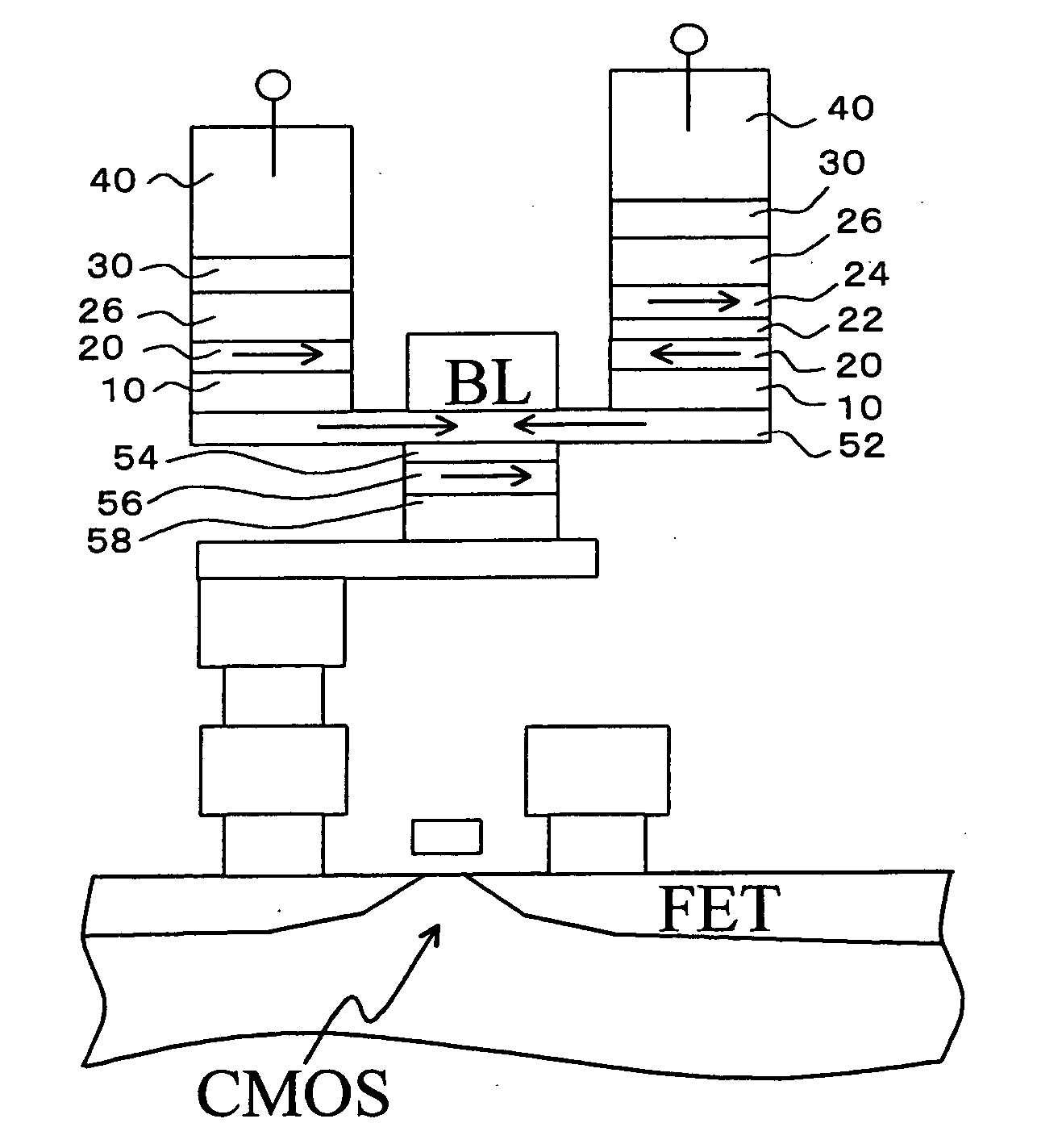
[0234] As the first example of the invention, one memory cell was fabricated on the basis of the memory array of the simple matrix structure shown in FIG. 18, the principle of the operation of the memory cell of the first type was confirmed.

[0235] It will be as the following if the structure of this magnetic memory is explained along with that manufacture procedure.

[0236] On the substrate which is not illustrated, a wiring layer with a thickness of 1 micrometer made of Cu was first produced by the damascene process as a lower layer bit line BL1. After that, an insulated layer was formed by CVD method, and then the surface was flattened by CMP (Chemical Mechanical Polishing).

[0237] Then, the stacking structure of TMR which has a ferromagnetic single tunnel junction structure was formed by a sputtering method. The material and the thickness of each layer were taken as Ta (10 nm) / Ru (3 nm) / Ir—Mn (8 nm) / CoFe (3 nm) / Ru (1 nm) / CoFe (3 nm) / AlOx (1 nm) / CoFeNi (2 nm) / Ru (5 nm) from the bo...

second example

[0245] Next, as the second example of the invention, one memory cell was fabricated on the basis of the memory array of the simple matrix structure shown in FIG. 20, the principle of the operation of the memory cell of the second type was confirmed.

[0246] It will be as the following if the structure of this magnetic memory is explained along with that manufacture procedure.

[0247] On the substrate which is not illustrated, a wiring layer with a thickness of 1 micrometer made of Cu was first produced by the damascene process as a lower layer bit line BL1. After that, an insulated layer was formed by CVD method, and then the surface was flattened by CMP (Chemical Mechanical Polishing).

[0248] Then, the stacking structure of TMR which has a ferromagnetic single tunnel junction structure was formed by a sputtering method. The material and the thickness of each layer were taken as Ta (2 nm) / Ru (3 nm) / Pt—Mn (12 nm) / CoFe (2.5 nm) / Ru (1 nm) / CoFe (3 nm) / AlOx (1 nm) / CoFeNi (1.8 nm) / Ru (1.5 n...


PUM


Abstract

A magnetic switching element includes: a ferromagnetic layer which is substantially pinned in magnetization in one direction; and a magnetic semiconductor layer provided within a range where a magnetic field from the ferromagnetic layer reaches, where the magnetic semiconductor layer changes its state from a paramagnetic state to a ferromagnetic state by applying a voltage thereto, and a magnetization corresponding to the magnetization of the ferromagnetic layer is induced in the magnetic semiconductor layer by applying a voltage to the magnetic semiconductor layer.

Description

CROSS-REFERENCE TO RELATED APPLICATIONS [0001] This application is based upon and claims the benefit of priority from the prior Japanese Patent Application No. 2001-397386, filed on Dec. 27, 2001; the entire contents of which are incorporated herein by reference. BACKGROUND OF THE INVENTION [0002] This invention relates to a magnetic switching element the and a magnetic memory, and more particularly, to the magnetic switching element which can generate magnetization in much lower power consumption than before by controlling a magnetization direction induced in a magnetic semiconductor, and the magnetic memory using the switching element. [0003] Magnetoresistance effect element using a magnetic film is used for the magnetic head, the magnetic sensor, for example, and there is a proposal to use the magnetoresistance effect elements in a solid-state magnetic memory (magnetoresistance effect memory or MRAM (Magnetic Random Access Memory)). [0004] Recently, a so called “tunneling magneto...

Claims


Application Information

Patent Timeline
IPC IPC(8): G01R33/09G11C11/14G11B5/39G11C11/15G11C11/16H01L21/8246H01L27/105H01L29/82H01L43/08
CPCG11C11/15G11C11/16H01L43/12H01L27/228H01L43/08H01L27/224G11C2213/74G11C2213/75G11C11/161G11C11/1675H10B61/10H10B61/22H10N50/10H10N50/01G11C11/18
Inventor SAITO, YOSHIAKI
Owner KK TOSHIBA
Why Eureka
Try Eureka