

Reconnectable chip interface and chip package
- Summary
- Abstract
- Description
- Claims
- Application Information
AI Technical Summary
Benefits of technology
Problems solved by technology
Method used
Image

Examples
Embodiment Construction
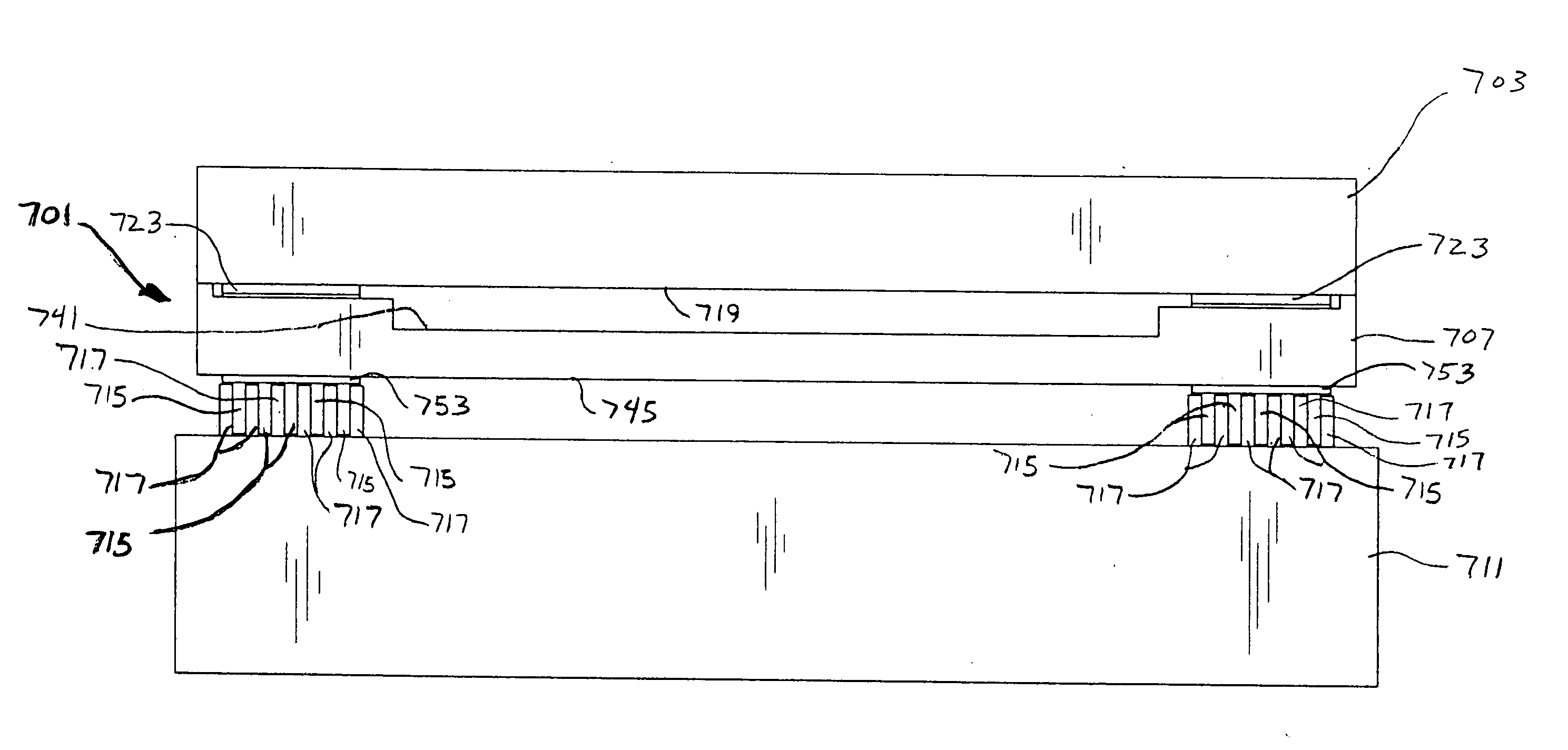
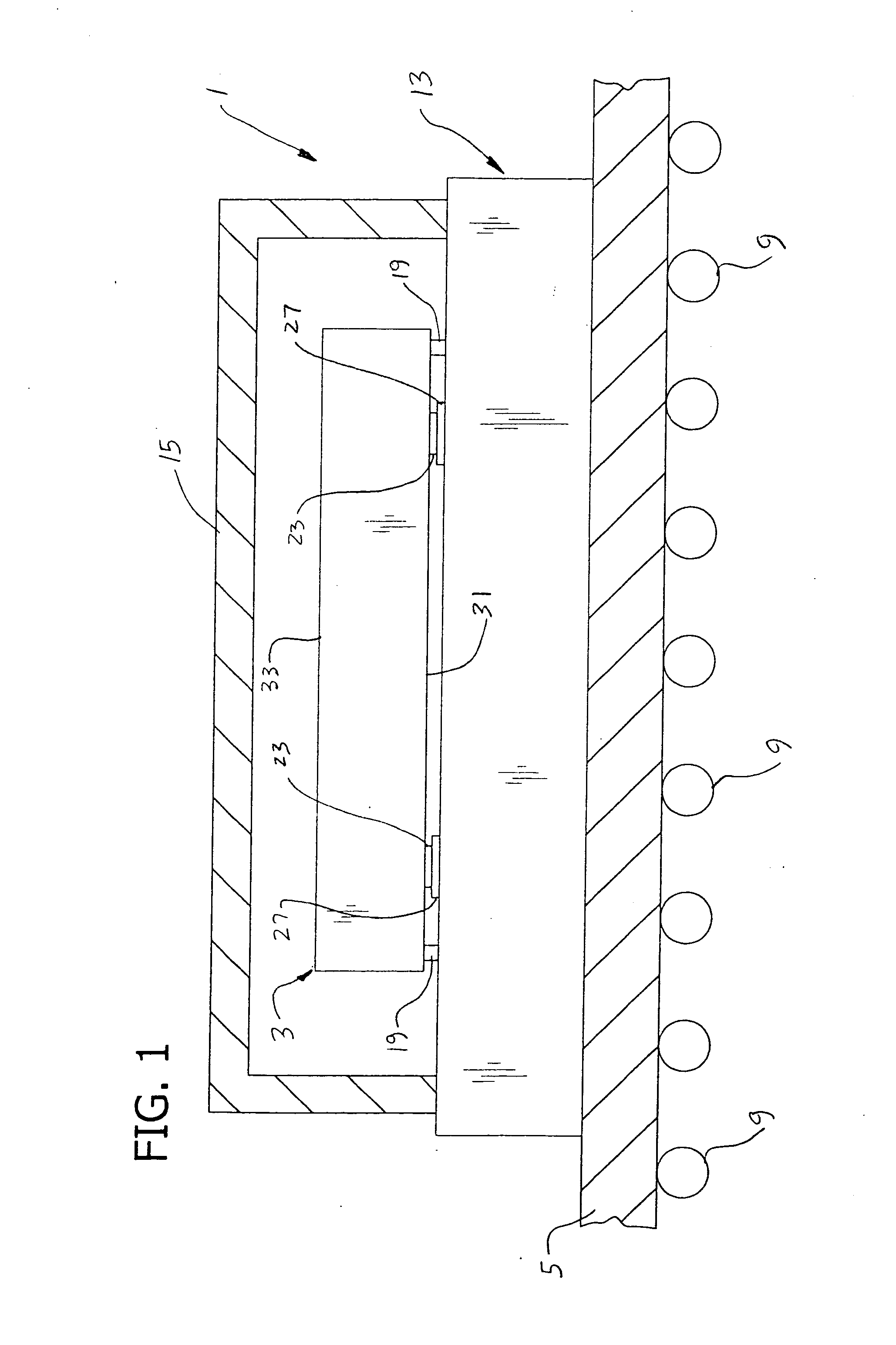
[0042] Referring now to the drawings, and more particularly to FIG. 1, a chip module, generally designated 1, comprises an integrated circuit device, generally designated 3, assembled in accordance with the present invention. In the particular embodiment of FIG. 1, the module 1 is affixed to a conventional ball grid array 5 having solder balls 9 for electrical connection to a printed circuit board (not shown). It will be understood that the chip module 1 could be directly attached to the circuit board or could be attached via other conventional connecting substrates (e.g., a pin-grid array or a land grid array). Also, the module 1 could include more than one integrated circuit device 3 assembled in accordance with the present invention.
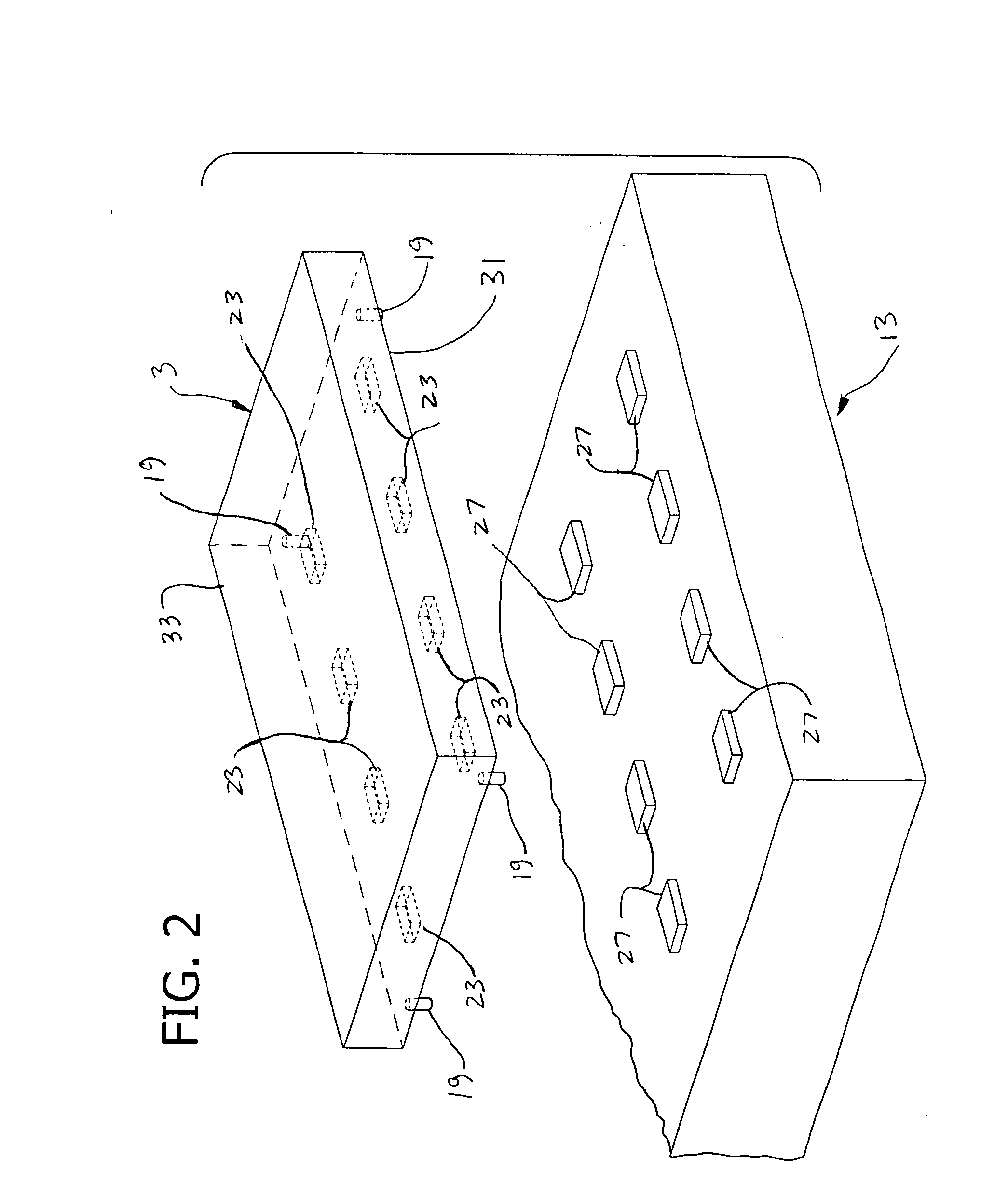
[0043] As shown in FIGS. 1 and 2, the integrated circuit device 3 of the module 1 is electrically and mechanically attached to a chip carrier substrate generally designated 13. In the illustrated embodiments, the circuit device 3 is shown schematical...
PUM
 Abstract
Description
Claims
Application Information