Light emitting device and method for fabricating light emitting device

a light emitting device and light emitting device technology, applied in the direction of instruments, discharge tube luminescnet screens, non-linear optics, etc., to achieve the effect of suppressing the potential drop of a counter electrode, high precision and precise pattern

Active Publication Date: 2005-01-20
SEMICON ENERGY LAB CO LTD
View PDF12 Cites 140 Cited by
  • Summary
  • Abstract
  • Description
  • Claims
  • Application Information

AI Technical Summary

Benefits of technology

[0016] According to the invention, an auxiliary electrode can be formed by using a photolithography since the auxiliary electrode is formed before forming a light emitting element. Further, a precise pattern can be formed by using the photolithography. Accordingly, even if the width between light emitting elements is reduced to less than 20 μm due to the high precision, the auxiliary electrode can be formed to fit within the width. Further, according to the invention, the auxiliary electrode is formed by photolith...

Problems solved by technology

Namely, an auxiliary electrode and a counter electrode are electrically connected in an a...

Method used


Image

  • Light emitting device and method for fabricating light emitting device
  • Light emitting device and method for fabricating light emitting device
  • Light emitting device and method for fabricating light emitting device

Examples


embodiment

[0044] Embodiment Mode 1

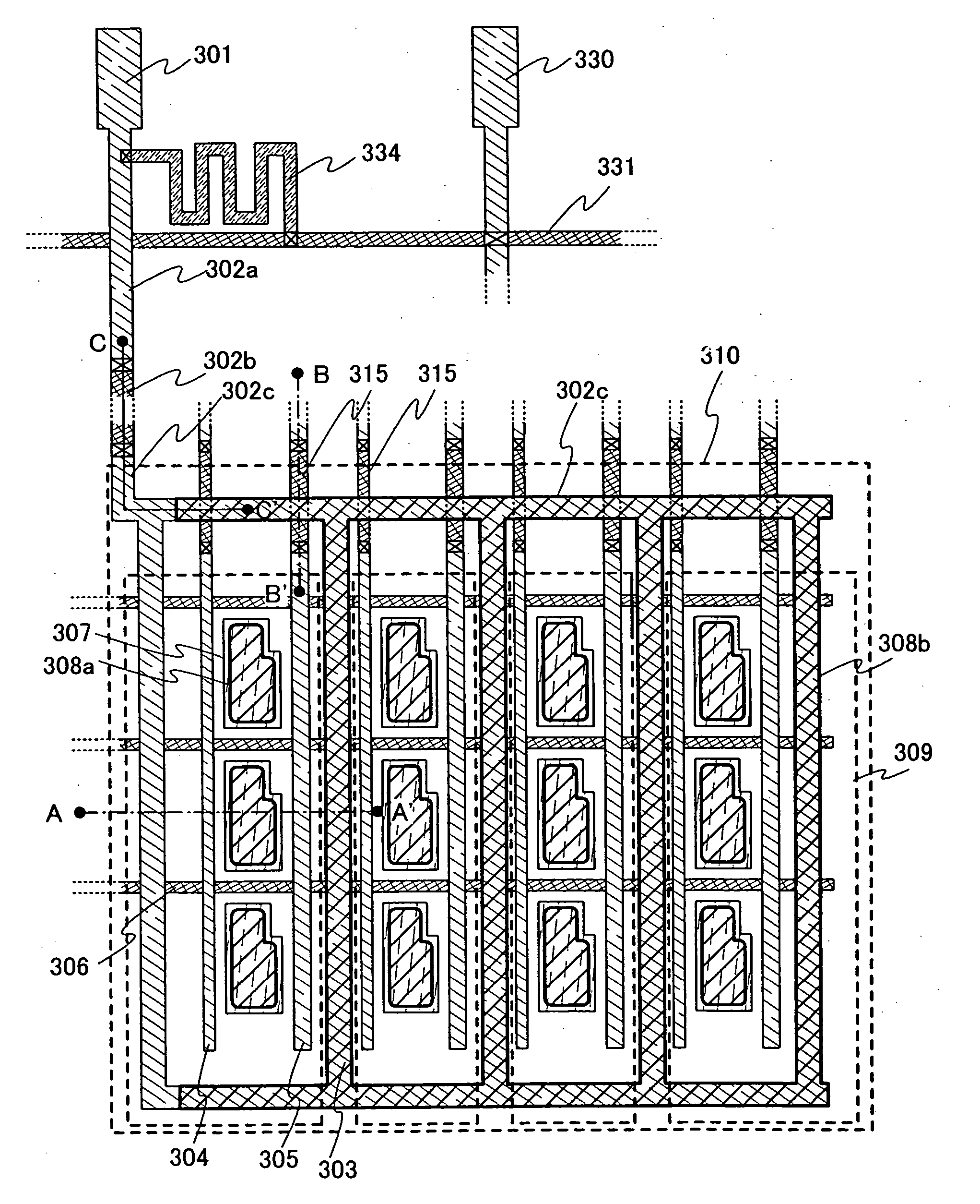
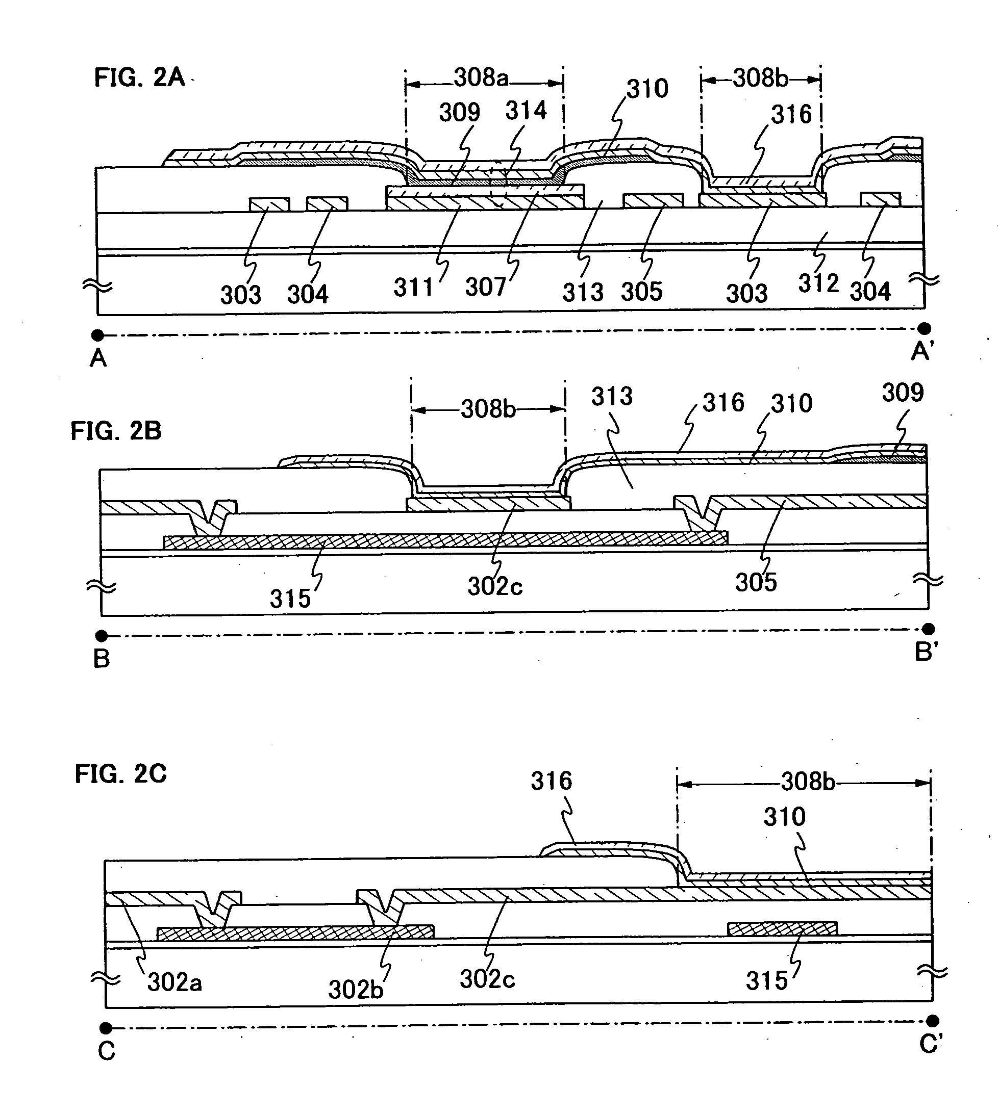
[0045] The configuration of a pixel area in a light emitting device of this embodiment mode will be described with reference to FIG. 1. FIG. 1 shows a top view of a pixel area and a leader wiring. Reference numeral 301 denotes a connection terminal, and reference numerals 302a, 302b, and 302c denote leader wirings. Further, an electrode 303 formed in the pixel area is equivalent to an auxiliary electrode, and the electrode is connected to the connection terminal 301 via the leader wirings 302a, 302b, and 302c. In FIG. 1, the connection terminal 301 and the auxiliary electrode 303 are electrically connected by using the three leader wirings of 302a, 302b, and 302c. However, the configuration of leader wirings is not limited to the configuration shown in FIG. 1, and any configuration may be used as long as the connection terminal 301 and the auxiliary electrode 303 can be connected electrically. All of a connection terminal, a leader wiring, and an auxiliary el...

embodiment 1

[0134] Embodiment 1

[0135] In this embodiment, a lay out of a leader wiring, an auxiliary electrode, a signal line, and a power line will be described.

[0136] A top view of a portion where a leader wiring and an auxiliary electrode are connected is shown in FIG. 15. Reference numeral 1201 denotes connection terminals, and the connection terminal is connected to a wiring 1203 via a wiring 1202. Further, the wiring 1203 is connected to a wiring 1205 via a wiring 1204. The wiring 1205 is connected to an auxiliary electrode 1206; more specifically, the wiring 1205 is formed with a conductive film shared by the auxiliary electrode 1206. Accordingly, in the case of FIG. 15, the leader wiring which connect the connection terminals 1201 and the auxiliary electrode 1206 are equivalent to the wirings 1202, 1203, 1204, and 1205.

[0137] Reference numeral 1207 denotes a signal line driver circuit, and the signal line driver circuit supplies a video signal to a signal line 1209 via a wiring 1208. ...

embodiment 2

[0139] Embodiment 2

[0140] In this embodiment, variations on a pixel of the invention will be described.

[0141]FIG. 16A shows an example of a pixel included in the light emitting device of the invention. The pixel shown in FIG. 16A has a light emitting element 901, a transistor used as a switching element for controlling a video signal inputted to the pixel, a driver transistor 903 for controlling a current value supplied to the light emitting element 901, and a current control transistor 904 for selecting whether current is supplied to the light emitting element 901 or not. The pixel may also have a capacitor element 905 for holding a potential of a gate of the transistor 904 as shown in this embodiment mode.

[0142] The switching transistor 902 may be either n-type or p-type. The driver transistor 903 and the current control transistor 904 may be either n-type or p-type, on condition that both of them has the same conductivity type. The driver transistor 903 is operated in a saturat...


PUM


Abstract

It is an object of the present invention to provide a method for fabricating a light emitting device, in which brightness gradient due to potential drop of a counter electrode can be prevented from being observed and an auxiliary electrode can be formed without increasing the number of steps, even when the precision of a light emitting device is improved. It is another object of the invention to provide a light emitting device fabricated according to the method. The light emitting device has a light emitting element and an auxiliary electrode in each pixel. The light emitting element includes a first electrode, a second electrode, an electroluminescent layer provided between the first and the second electrodes. Further, the first electrode is overlapped with the electroluminescent layer and the second electrode formed over an insulating film by means of a first opening formed in the insulating film. Still further, the auxiliary electrode is overlapped with the second electrode by means of a second opening formed over the second insulating film.

Description

BACKGROUND OF THE INVENTION [0001] 1. Field of the Invention [0002] The present invention relates to a light emitting device in which a light emitting element and an element for supplying current to the light emitting element are provided for each of a plurality of pixels and to a method for fabricating the light emitting device. [0003] 2. Description of the Related Art [0004] A light emitting element has high visibility since it emits light by itself, and is most suitable for thinning since it does not need a backlight, which is required in a liquid crystal display device (LCD); further, there is no limitation of viewing angle either. Therefore, a light emitting device with the use of a light emitting element has been attracting attention as a display device which replaces a CRT and an LCD. In late years, a light emitting device has been put to practical use; for example, it is provided in a cellular phone or an electronic device such as a digital still camera. [0005] A light emitt...

Claims


Application Information

Patent Timeline
IPC IPC(8): H01L27/32H01L51/50H01L51/52H05B33/00H05B44/00
CPCH01L27/3246H01L27/3248H01L27/3276H01L2251/5315H01L51/5203H01L51/5221H01L51/5092G02F1/136204H10K59/122H10K59/123H10K59/1315H10K50/171H10K2102/3026H10K59/805H10K59/80522H10K59/80524H10K50/828H10K50/824H10K50/805
Inventor YAMAZAKI, SHUNPEINAGAO, RITSUKONAKAMURA, YASUO
Owner SEMICON ENERGY LAB CO LTD
Why Eureka
Try Eureka