Monolithic ceramic electronic component

a technology of electronic components and monolithic ceramics, applied in the direction of fixed capacitor details, magnetic bodies, fixed capacitors, etc., can solve the problem of difficult to reach magnetization saturation, achieve low dielectric constant, improve impedance characteristics, and reduce variations in electromagnetic characteristics

Active Publication Date: 2005-01-20
MURATA MFG CO LTD
View PDF5 Cites 10 Cited by
  • Summary
  • Abstract
  • Description
  • Claims
  • Application Information

AI Technical Summary

Benefits of technology

[0013] A monolithic ceramic electronic component according to a preferred embodiment of the present invention has a low dielectric constant because of its porous ceramic body. As a result, impedance characteristics are improved at high frequencies, and variations in electromagnetic characteristics decrease. Furthermore, when a direct current is superimposed, the monolithic ceramic electronic component has a small variation in self-resonant frequency and has a rate of decrease in impedance of about 50% or less.
[0014] Since magnetic grains are discontinuously disposed due to the pores in the ceramic body, the movement of magnetic domain walls induced by a magnetic field produced by a current is blocked. As a result, magnetization saturation is difficult to reach. Hence, the impedance characteristics are improved, and a variation in self-resonant frequency decreases. In addition, at least approximately 40 percent of the total volume of the pores is filled with a resin. Curing the resin produces residual stress, causing strain that prevents magnetic saturation. Consequently, the decrease in impedance with the superimposed direct current is suppressed.

Problems solved by technology

As a result, magnetization saturation is difficult to reach.

Method used


Image

  • Monolithic ceramic electronic component
  • Monolithic ceramic electronic component
  • Monolithic ceramic electronic component

Examples


Embodiment Construction

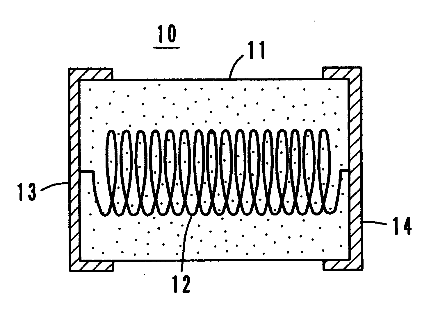
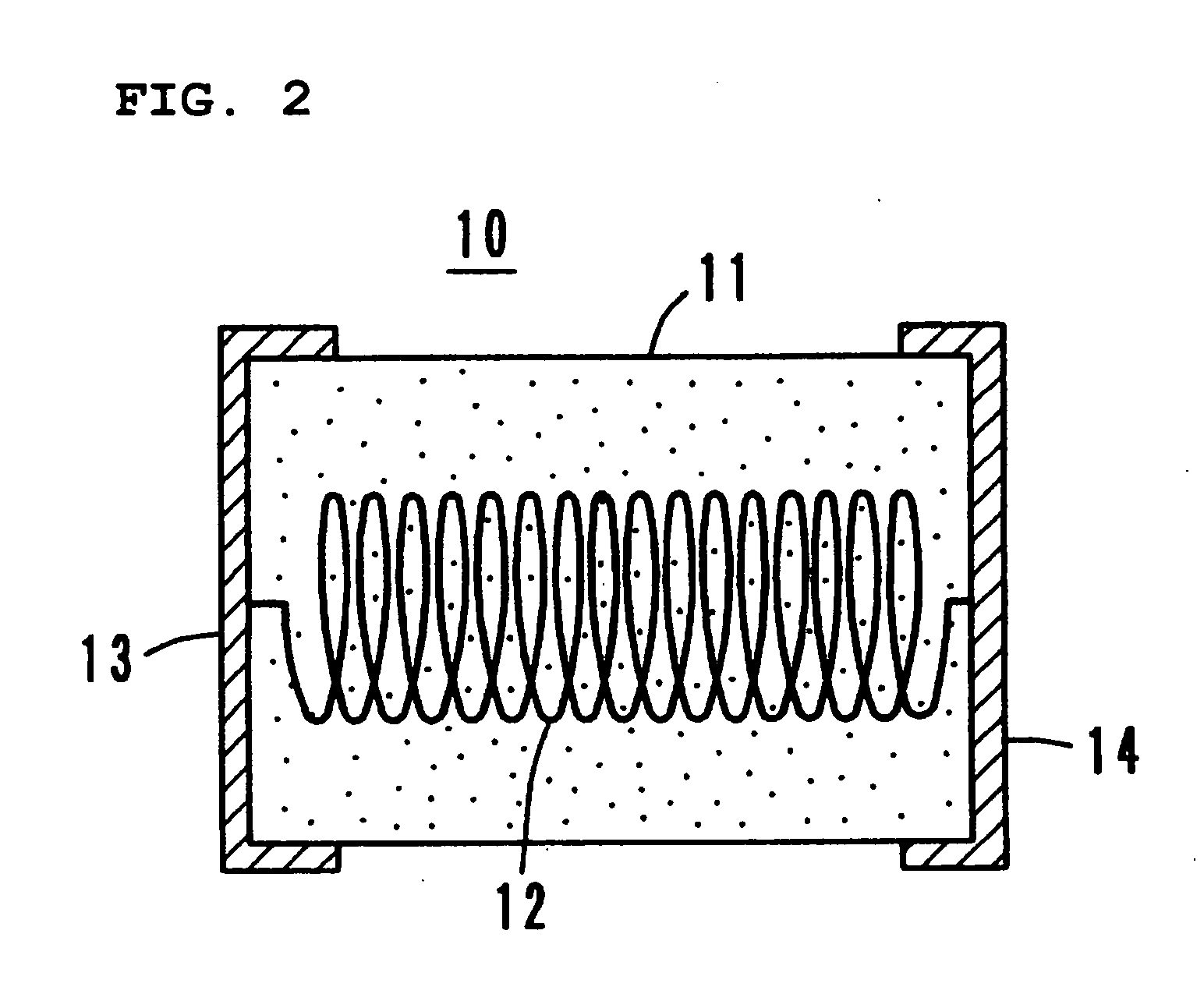
[0028] A preferred embodiment of a monolithic ceramic electronic component according to the present invention will now be described below with reference to the drawings.

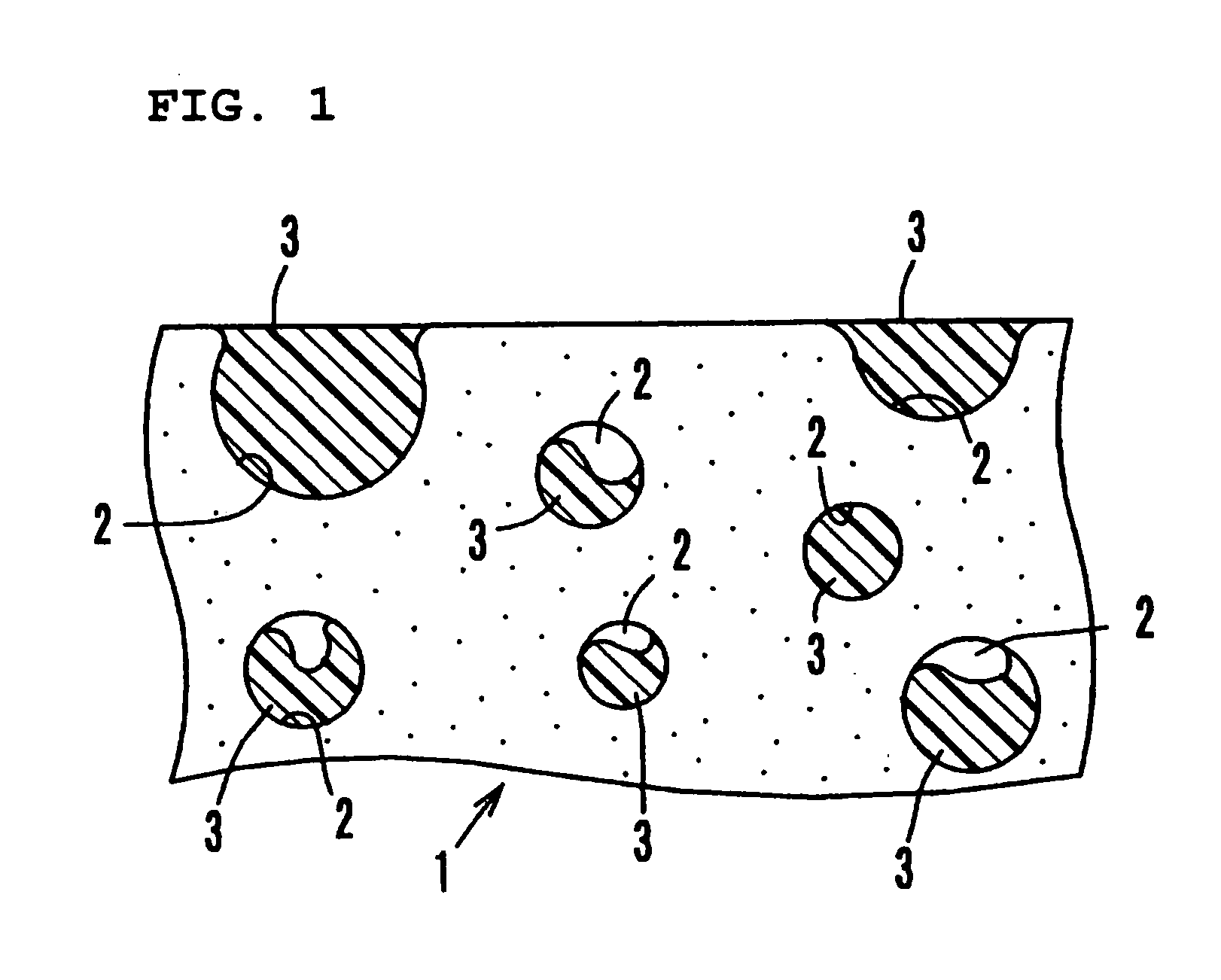
[0029] Referring to FIG. 1, a sintered ceramic constituting the monolithic ceramic electronic component will be described.

[0030] A plurality of pores 2, which are filled with a resin 3, are provided in a sintered ceramic 1. The pores 2 preferably have an average diameter of about 5 μm to about 20% m. The pores 2 also have two structures, that is, open pores and closed pores. The sintered ceramic 1 preferably has a porosity of greater than about 30 percent and less than about 80 percent by volume. In the monolithic ceramic electronic component according to a preferred embodiment of the present invention, at least approximately 40 percent of the total volume of the pores 2 are filled with the resin 3.

[0031] To evaluate the effect of the pores and the resin, samples 1 to 6 (chip inductors) were manufactured. Sample 1...


PUM

PropertyMeasurementUnit
porosityaaaaaaaaaa
diameteraaaaaaaaaa
dielectric constantaaaaaaaaaa

Abstract

A sintered ceramic has a porosity of greater than about 30 percent and less than about 80 percent by volume. Pores are filled with an epoxy resin. A filling factor of the epoxy resin is about 40 percent by volume or more. A monolithic ceramic electronic component having an inner electrode, for example, a chip inductor is manufactured with such a porous sintered ceramic. When a direct current is superimposed, the resulting monolithic ceramic electronic component has a substantially unchanged self-resonant frequency and also has a rate of decrease in impedance of about 50 percent or less at 100 MHz.

Description

BACKGROUND OF THE INVENTION [0001] 1. Field of the Invention [0002] The present invention relates to monolithic ceramic electronic components, and more particularly, the present invention relates to inductors, LC combined electronic components, LR combined electronic components, and LCR combined electronic components, which can operate at high frequencies. [0003] 2. Description of the Related Art [0004] In recent years, electronic devices operating at high frequencies have become common. Inductors, LC combined components, LR combined components, LCR combined components, and the like, which can operate at gigahertz (GHz) frequencies, have become necessary. [0005] However, in an inductor for high-frequency operation, stray capacitance occurring in parallel with the inductor seriously affects the impedance of the inductor. In particular, at GHz frequencies, small stray capacitance, in the range of 0.01 pF to 0.1 pF, seriously affects the impedance. Consequently, to achieve the desired ...

Claims


Application Information

Patent Timeline
Patent Type & Authority Applications(United States)
IPC IPC(8): H01G4/12H01C7/18H01F1/34H01F1/37H01F17/00H01F17/04H01F41/04H01G4/30H01G4/40
CPCH01F1/344H01F1/37H01F17/0013Y10T428/24926H01F41/046H01F2017/048H01F17/0033Y10T428/249956H01C7/18
Inventor TAKAZAWA, TOMOOOTSUKI, TAKEHIKOKAWABATA, TOSHIOTACHIBANA, KAORU
Owner MURATA MFG CO LTD
Why Eureka
Try Eureka