

Light-emitting material and light-emitting device
a technology of light-emitting material and light-emitting device, which is applied in the direction of luminescnet screen, discharge tube luminescnet, natural mineral layered products, etc., can solve the problem of insufficient description of the low luminous efficiency of the elements, and difficulty in considering the sufficient utilization of the properties of the copper complexes. achieve high luminous efficiency and high stability
- Summary
- Abstract
- Description
- Claims
- Application Information
AI Technical Summary
Benefits of technology
Problems solved by technology
Method used
Image

Examples
examples 1 to 10
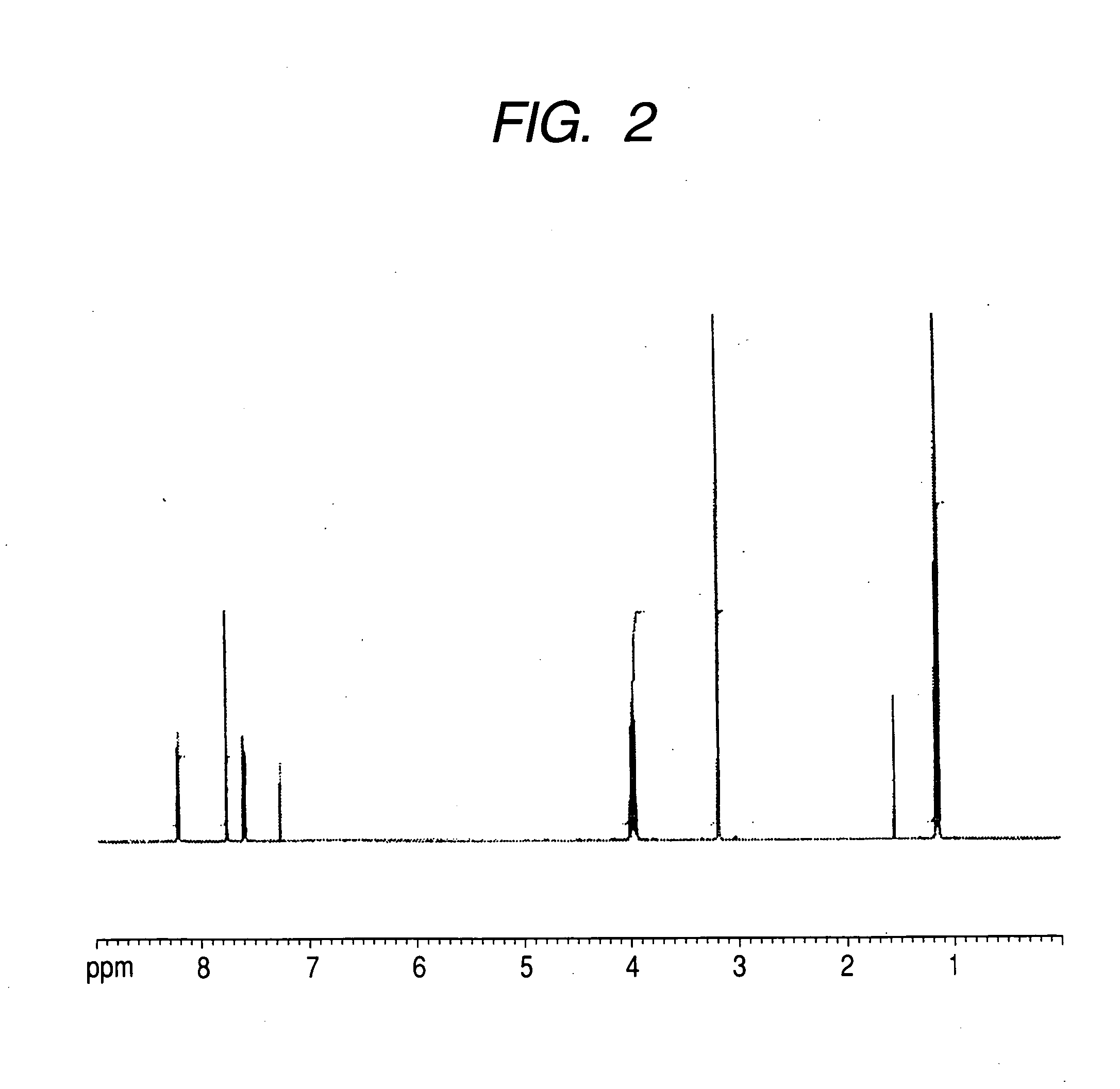
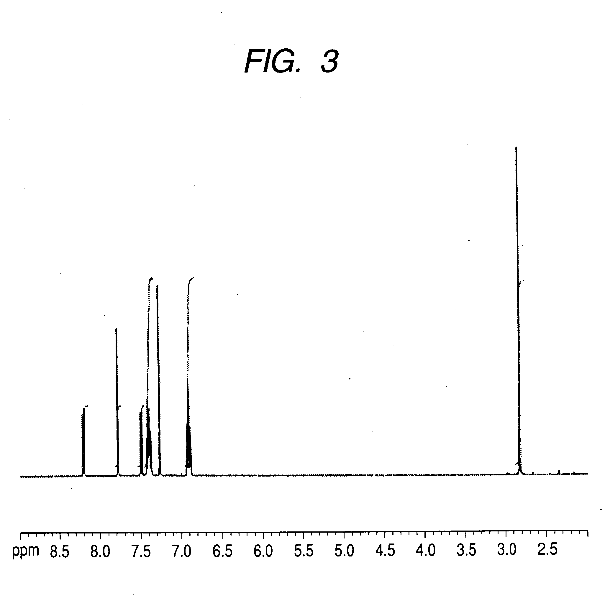
Compounds listed in Table 10 were synthesized according to the formula (A). Their structures were identified through 1H-NMR (Bruker DPX-400 NMR) and elemental analysis (Vario EL CHNOS). FIGS. 2 and 3 show 1H-NMR charts of Exemplified Compounds 326 and 335, respectively. Elemental analyses of the compounds agreed well with the calculated values for their weight ratios of elements C, H, and N.
In addition, their light-emitting properties by photoexcitation were measured. Table 10 shows the results. Their emission spectra were measured by using an F4500 (manufactured by Hitachi Instruments Service Co., Ltd., having an excitation wavelength in the range of 380 to 450 nm). The measurement was performed while all the compounds were in powder states. Their luminescent colors ranged from yellowish orange to red.
TABLE 10Light emissionExemplifiedspectrum peakExampleCompound No.λmax (nm)11015932102610313860842515925274605632660173326208335578936360010368592
Strong light emission was obtain...
examples 11 and 12
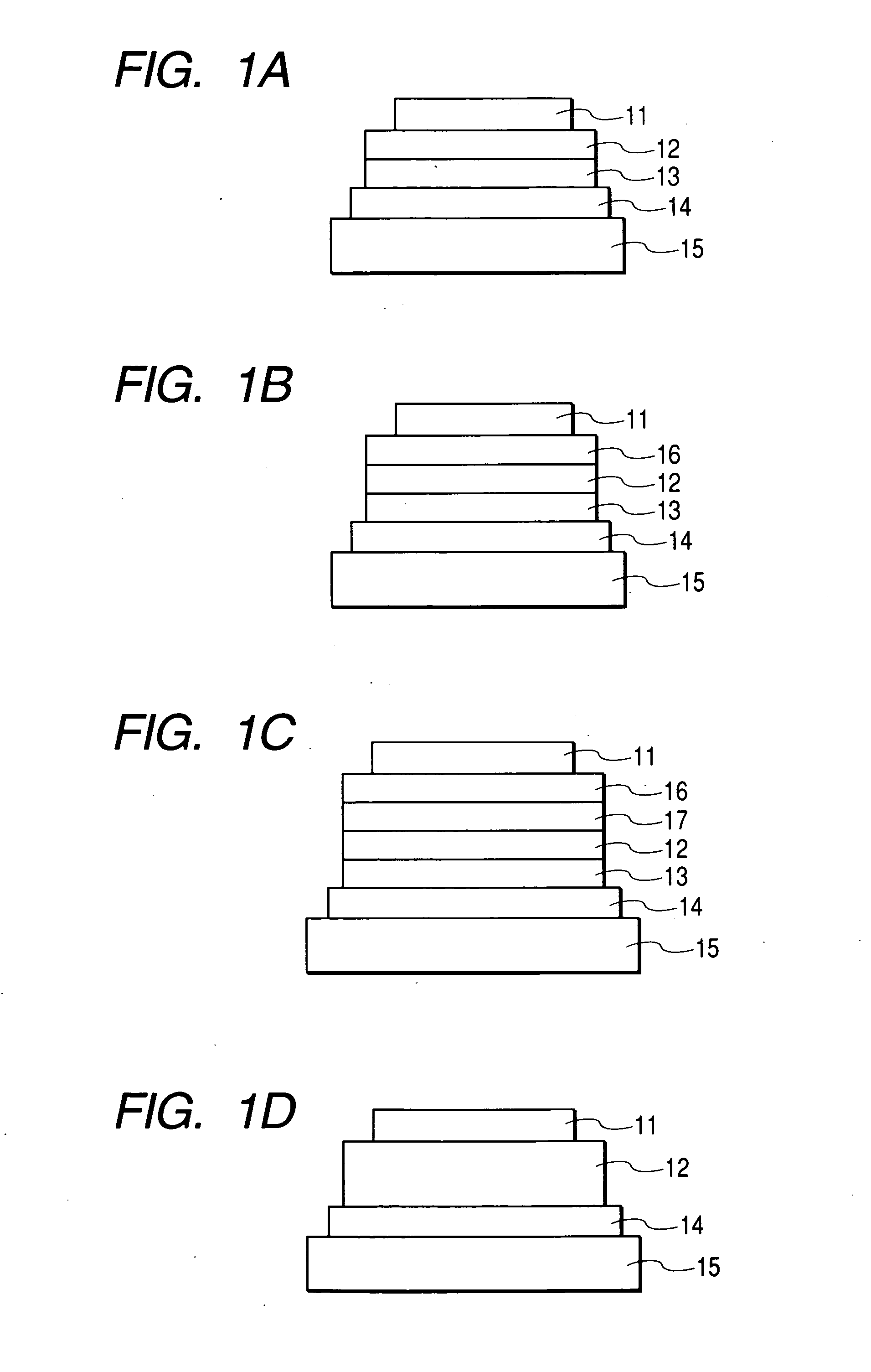
In each example, an organic EL element was prepared by using Exemplified Compound 101 synthesized in Example 1 or Exemplified Compound 102 synthesized in Example 2 as a light-emitting material.
The element construction employed was one having only one organic layer as shown in FIG. 1D. ITO of 100 nm in thickness (corresponding to the transparent electrode 14) was patterned on a glass substrate (corresponding to the transparent substrate 15) to have an electrode area of 3 mm2.
An organic layer of 120 nm in thickness (corresponding to the light-emitting layer 12) was formed on the ITO substrate by spin-coating a solution containing the following compounds under a nitrogen atmosphere at 2,000 rpm for 20 seconds.
Chlorobenzene:10gPolyvinyl carbazole (having an average molecular100mgweight of 9,600):Exemplified Compound 101 or 102:3.0mg
After the film formation, the substrate was loaded into a vacuum evaporation chamber to form a cathode having the following construction (correspondi...
examples 13 and 14
In each example, a single bit organic EL element shown in FIG. 1B having three organic layers consisting of the hole-transporting layer 13, the light-emitting layer 12, and the electron-transporting layer 16 was prepared by using Exemplified Compound 101 synthesized in Example 1 or Exemplified Compound 251 synthesized in Example 4. Then, the element properties were measured.
A no alkali glass substrate was used as the transparent electrode 15. Then, indium tin oxide (ITO) of 100 nm in thickness was formed as the transparent electrode 14 on the transparent substrate 15 according to a sputtering method, and was patterned into an electrode of 2 mm in diameter.
A high molecular weight film solution containing PEDOT and PSS represented by the above structural formulae was spin-coated on the transparent electrode 14 to form the hole-transporting layer 13 of 30 nm in thickness. A 1.0% chloroform solution of each of Exemplified Compounds 101 and 251 was spin-coated twice on the hole-tra...
PUM
| Property | Measurement | Unit |
|---|---|---|
| structure | aaaaa | aaaaa |
| stability | aaaaa | aaaaa |
| temperature | aaaaa | aaaaa |
Abstract
Description
Claims
Application Information