Process kit for erosion resistance enhancement

a technology of erosion resistance and process kit, which is applied in the direction of electrical equipment, basic electric elements, electric discharge tubes, etc., can solve the problems of substantial prolongation of the life of the process kit, and achieve the effect of minimizing the impact of the coefficient of thermal expansion (cte) difference, minimizing the effect of temperature variation on the polymer layer, and limited thickness

Inactive Publication Date: 2005-01-27
APPLIED MATERIALS INC
View PDF7 Cites 46 Cited by
  • Summary
  • Abstract
  • Description
  • Claims
  • Application Information

AI Technical Summary

Benefits of technology

[0016] In a third aspect of the invention, the layer of fluorocarbon-based polymer is controlled to be thin, e.g., 1.5 mm, so as to minimize the impact of the Coefficient of the Thermal Expansion (CTE) difference between the

Problems solved by technology

Therefore, this layer effectively insulates the process kit from erosion by the react

Method used


Image

  • Process kit for erosion resistance enhancement
  • Process kit for erosion resistance enhancement
  • Process kit for erosion resistance enhancement

Examples


Embodiment Construction

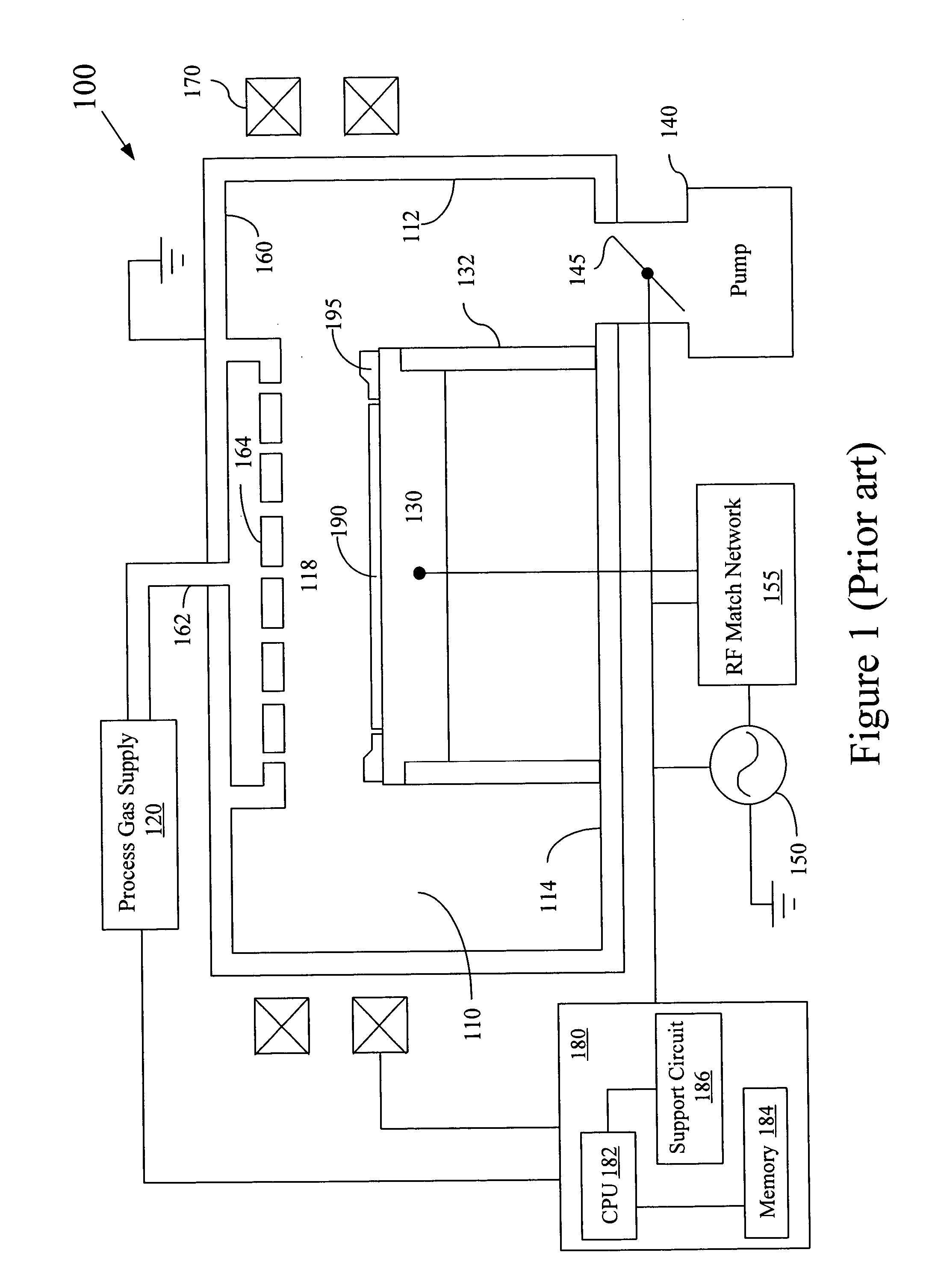
[0022] The process kit of the present invention provides a uniform plasma ion and plasma energy distribution across the top surface of a semiconductor wafer. The process kit of the present invention resists erosion caused by the highly reactive species in the plasma and thereby significantly prolongs its lifetime to achieve higher production throughput and lower production consumable cost. The process kit of the present invention can be deployed in a plasma reactor, such as, for example, the Dielectric Etch eMAX System, the Dielectric Etch Super eCentura System, or the Centura MxP Dielectric Etch system, all of which are commercially available from Applied Materials Inc., Santa Clara, Calif.

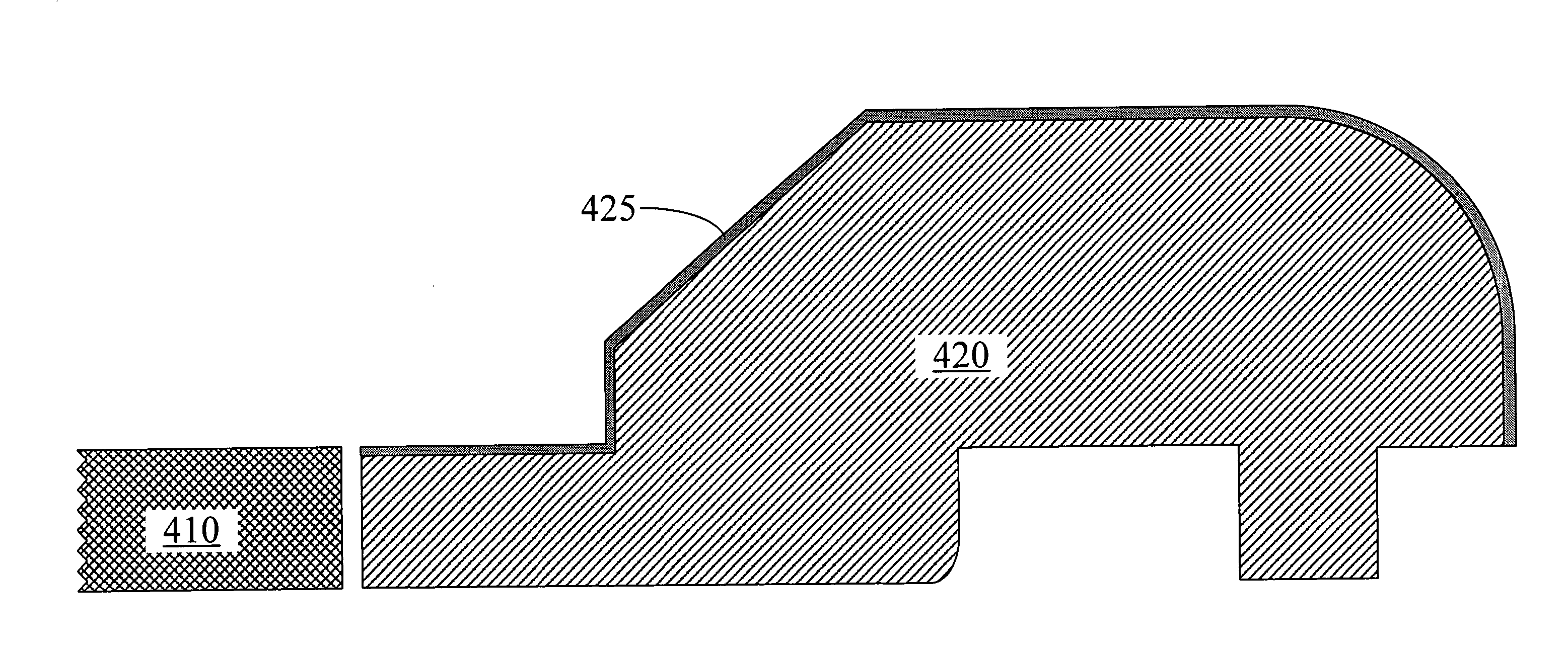
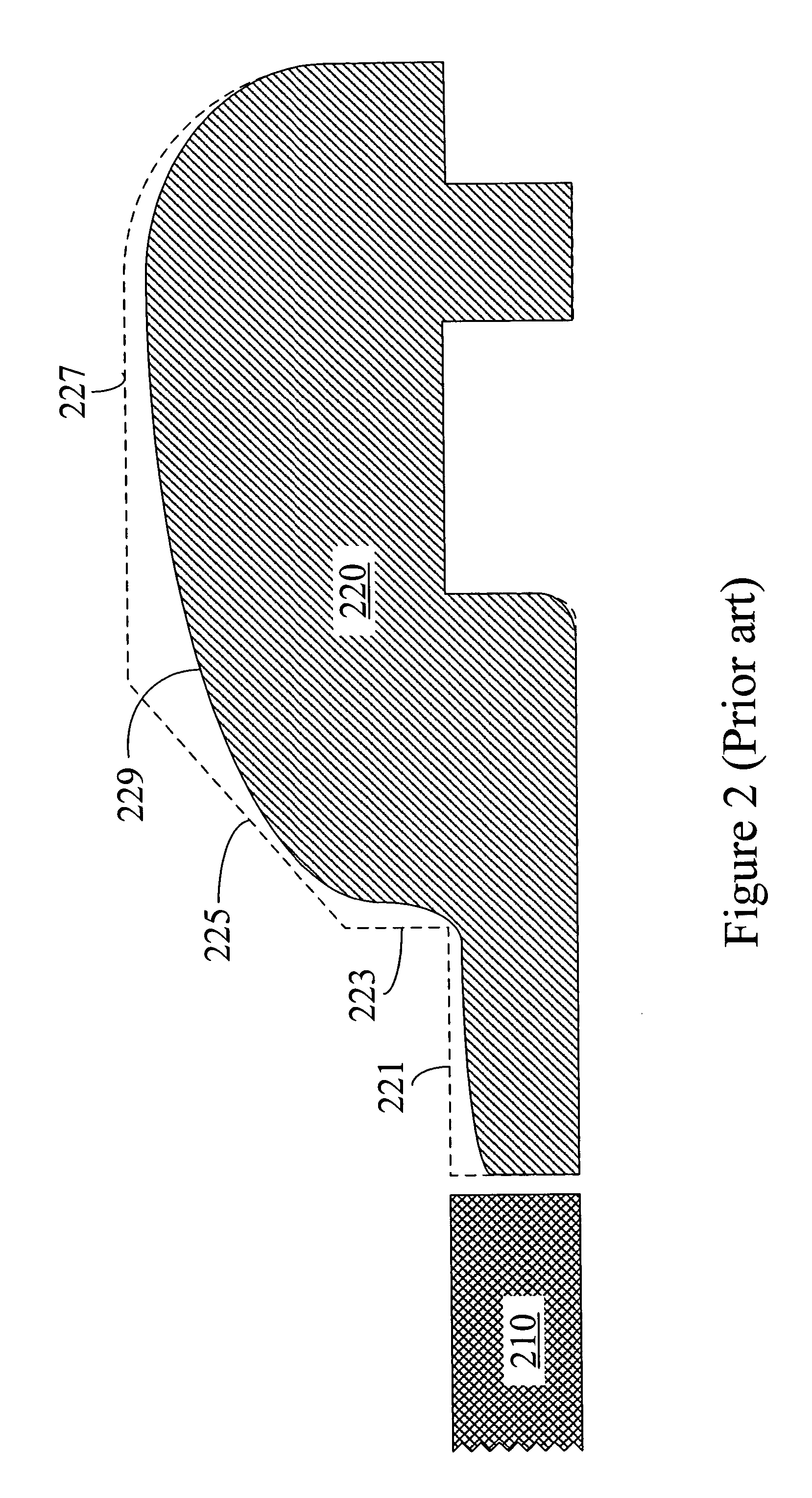
[0023]FIG. 3 provides a sectional view of pedestal 130, wafer 190, and conventional process kit 195 of FIG. 1 with more details. Wafer 190 is secured at the center of the pedestal by an electrostatic chuck (not shown), or e-chuck. The e-chuck is supported by a dielectric member 390 having a cath...


PUM

PropertyMeasurementUnit
Thicknessaaaaaaaaaa
Thicknessaaaaaaaaaa
Electrical resistanceaaaaaaaaaa

Abstract

A process kit is described that resists plasma erosion, preserves the spatial uniformity of plasma properties, reduces particle generation in the chamber, and significantly enhances the lifetime of the process kit. A layer of polymer material covers the top surface of the process kit. The polymer material is fluorocarbon-based and not reactive with the species in the plasma. The polymer material not only protects the process kit from progressive erosion, but also prevents the generation of particles in the chamber. The polymer material has similar permittivity to that of the process kit and therefore maintains the spatial uniformity of plasma properties, e.g., etch rate, near the wafer perimeter. The thickness of the layer is controlled between 0.5 and 1.5 mm such that the difference between its coefficient of thermal expansion and that of the process kit will not cause the layer to peel off the process kit's top surface.

Description

FIELD OF THE INVENTION [0001] The present invention generally relates to a process kit surrounding a semiconductor workpiece in a plasma chamber that can improve the spatial uniformity of plasma energy distribution over the workpiece surface. More specifically, the present invention relates to a film of fluorocarbon-based polymer covering the top surface of the process kit that can resist plasma-related erosion, reduce particulate contamination during etching, and prolong the lifetime of the process kit. BACKGROUND OF THE INVENTION [0002] Semiconductor fabrication includes a series of processes that produce numerous identical integrated circuits in a semiconductor workpiece, e.g., a silicon wafer, in accordance with a circuit design. One important process is plasma etching, which is a process of transferring a pattern in a layer of mask material into another layer under the mask, such as a layer of conductive or dielectric material, by removing the layered material from the wafer su...

Claims


Application Information

Patent Timeline
IPC IPC(8): H01J37/32H01L21/3065
CPCH01J37/32642H01J37/32477H01L21/3065
Inventor SUN, JENNIFER Y.KUMAR, ANANDA H.THACH, SENH
Owner APPLIED MATERIALS INC
Why Eureka
Try Eureka