Structure of multi-tier wire bonding for high frequency integrated circuit

a high-frequency integrated circuit and multi-tier wire bonding technology, applied in the structure field, can solve the problems of affecting the performance of the package, the return loss of the bond-wire structure is usually less than 15 db, and the limit of the signal loop, so as to improve the high frequency response of the circuit, reduce the loss of the insertion of the chip, and reduce the loss of the insertion. loss

Active Publication Date: 2005-01-27
VIA TECH INC
View PDF1 Cites 53 Cited by
  • Summary
  • Abstract
  • Description
  • Claims
  • Application Information

AI Technical Summary

Benefits of technology

[0012] In conclusion, this invention provides a structure and method of multi-wire wire bonding suitable for a high frequency signal. By adding grounding wires at the surrounding area of the signal wire, and connecting part of the grounding wires to the chip carrier (die pad), the return loss and the impedance matching are increased, the insertion loss of the chip is reduced, and the high frequency response of the circuit is improved

Problems solved by technology

However, as the operating frequency moves beyond several giga-hertz, the parasitic inductance and the parasitic capacitance induced by the bonding wire will significantly impact the circuit performance and can no longer be neglected.
Since the lead-frame pitch is usually larger than 0.5 mm, the ends of the bonding wires are much far apart each other and hence the reduction of the signal loop is limited.
As a result, the return loss of this bond-wire structure is usually less than 15 dB at 5 GHz since the decrease of the loop inductance is still not large enough.
However, although the conventional bonding structure shown in FIG. 2 can shorten the grounding path of the die 240, the arrangement of the bonding wires, i.e. 270, 273, 275, and 277, will still generate electromagnetic interference and hence affect the performance of the package.

Method used


Image

  • Structure of multi-tier wire bonding for high frequency integrated circuit
  • Structure of multi-tier wire bonding for high frequency integrated circuit
  • Structure of multi-tier wire bonding for high frequency integrated circuit

Examples


Embodiment Construction

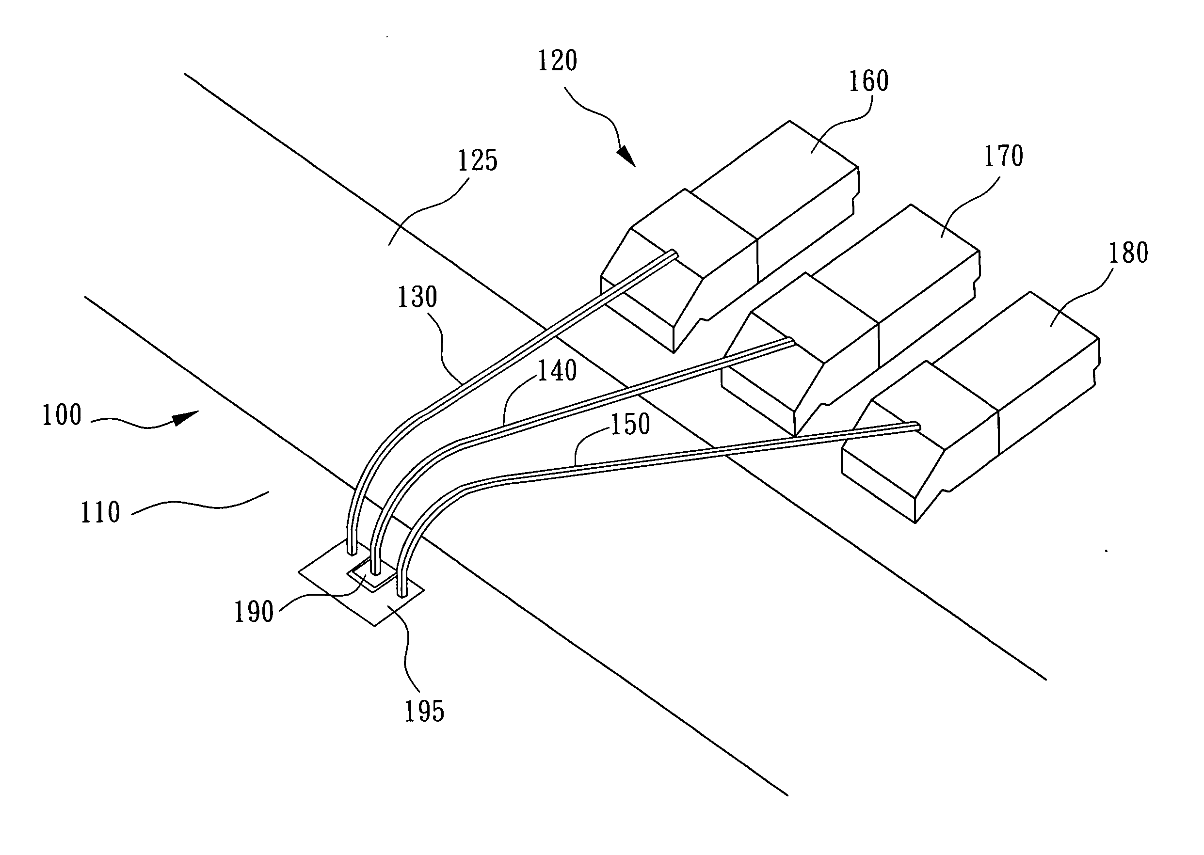
[0021] Because the conventional bonding structure generates big parasitic inductance, and electromagnetic interference (noise), this invention does not only use a coplanar bonding pad on the IC chip, but also bonding the grounding wires of the coplanar bonding pad to the die pad below the chip in order to shorten the path of the grounding. This invention also adding the grounding wires bonding to the die pad and has a better arrangement of the grounding wires in order to decrease the insertion loss and increase the return loss and to improve the electrical characteristic of the bonding structure.

[0022] This invention provides a structure and method of multi-wire wire bonding that there are coplanar bonding pads at the chip. Part of the grounding wires connect to the die pad, part of the grounding wires connect to the lead frames. In addition, the number of the grounding wires is increased.

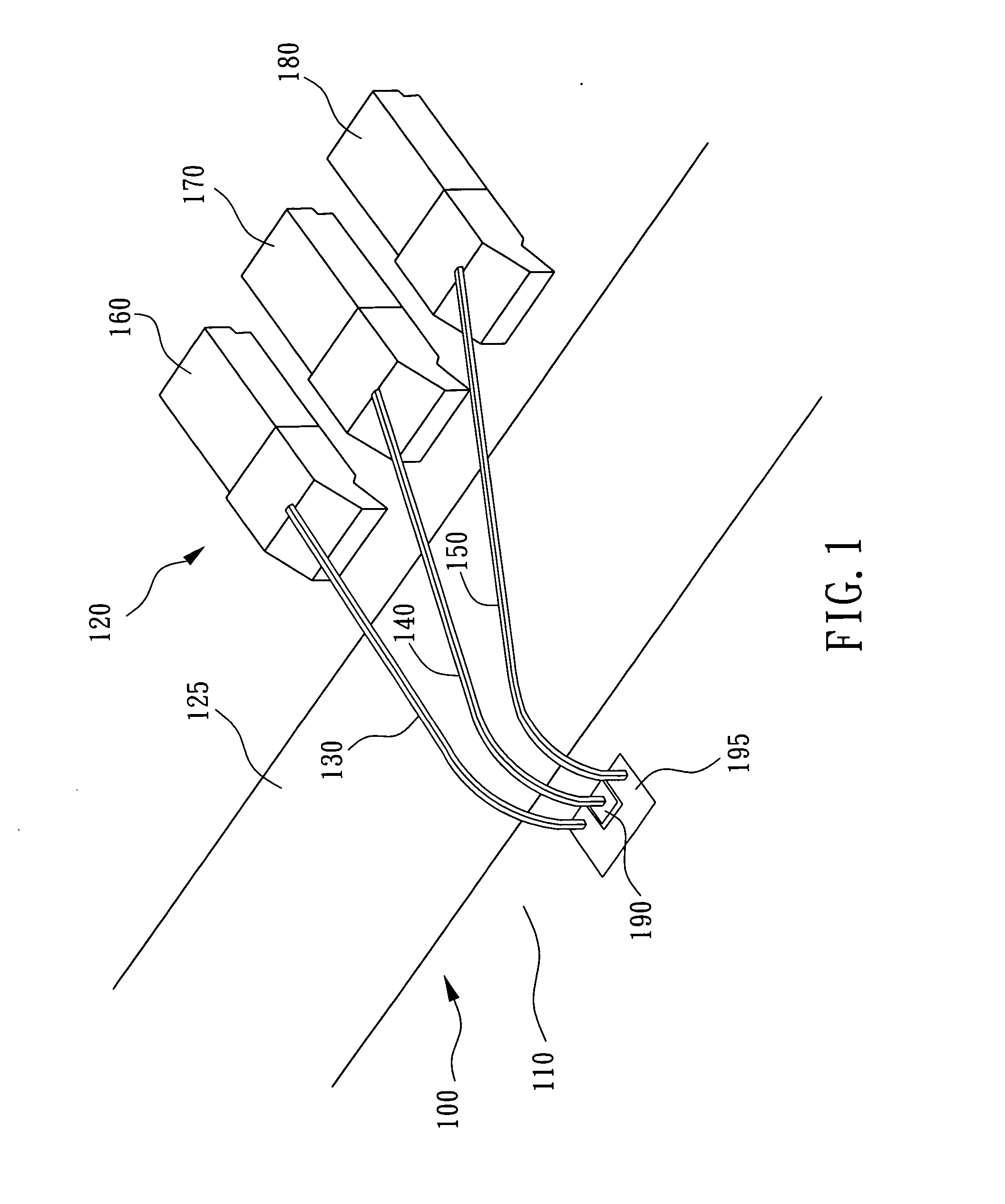
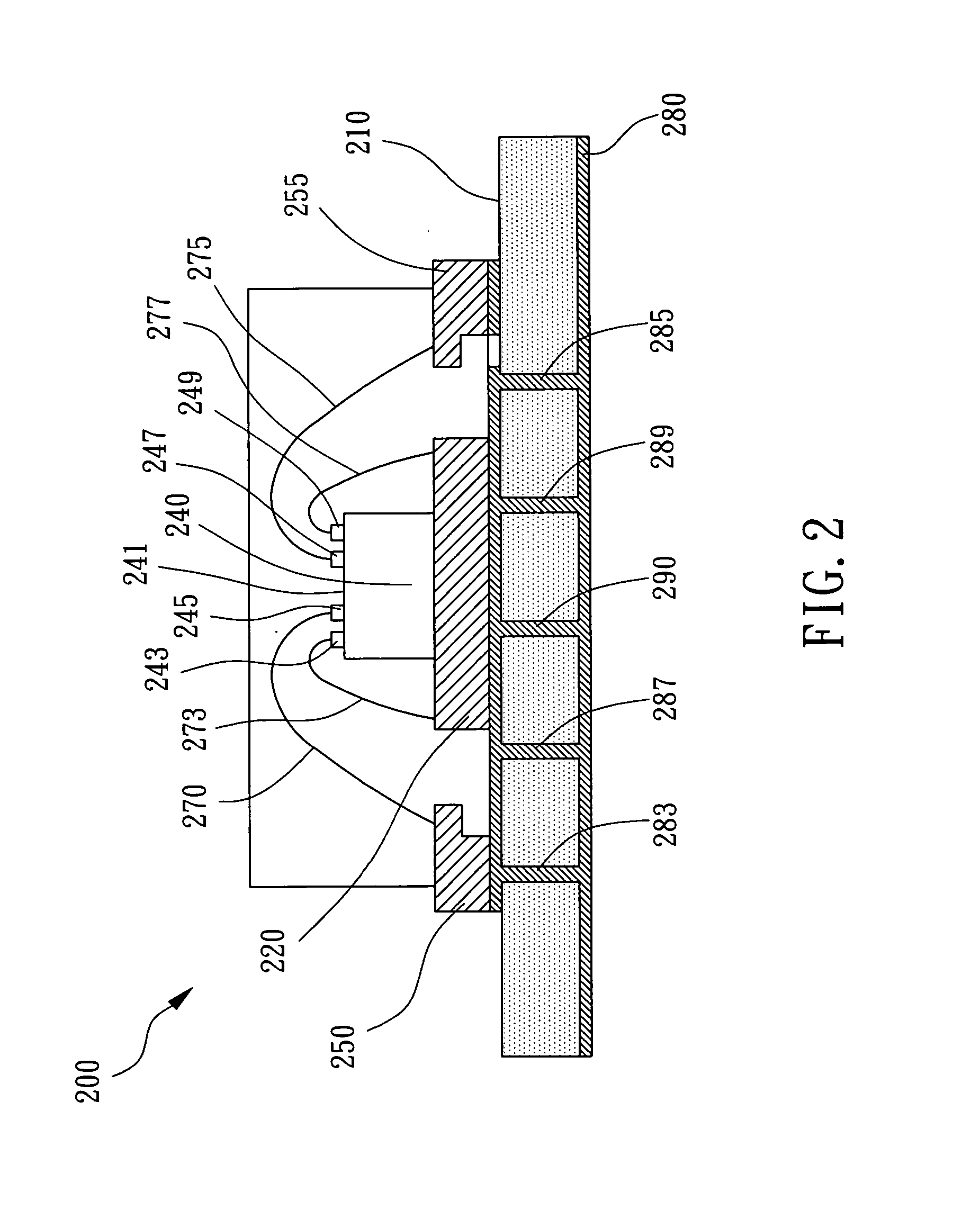
[0023] Please refer to FIGS. 3A and 3B. FIGS. 3A and 3B demonstrated the top-view and 3D diag...


PUM


Abstract

A multi-wire wire-bonding structure suitable for a high frequency signal comprises a first electronic device, a second electronic device, a chip pad and a plurality of metal wires. The first electronic device is attached to the second electronic device with the chip pad. As a result, the first electronic device and the second electronic device form a stair-like structure. A plurality of bonding pads comprises at least one signal bonding pad and grounded bonding pads. The signal bonding surface is surrounded by the ground bonding pads. All the bonding pads are located at the surface of the first electronic device. The chip pad carries the first electronic device and the exceeding part is a ring grounded bonding pad which surrounds the first electronic device. The second electronic device carries the chip pad and a margin of the second electronic device is exceeding the chip pad. There are several leads on the margin of the second electronic device in corresponding to the ground bonding pads and the signal bonding pad. Metal wires comprise a signal wire and grounding wires. The bonding pads of the first electronic device are classified as the first row bonding pads which is close to the ring ground bonding surface and the second row bonding pads which is away from the ring ground bonding surface. The signal wire electrically connects to the signal bonding pads and the corresponding lead. The ground wires electrically connect to the first row bonding pads and the ring ground bonding surface.

Description

FIELD OF THE INVENTION [0001] The present invention relates to a structure and a method of multi-tier wire bonding for high frequency integrated circuit, and more particular, to a structure and a method of multi-tier wire bonding for high frequency integrated circuit capable of optimizing the electrical connection between electronic devices. DESCRIPTION OF THE PRIOR ARTS [0002] Bond-wires are extensively used in the integrated circuit packaging for the interconnection between the die and the lead frames or the fingers on the printed circuit board (PCB) since they are inexpensive and robust. However, as the operating frequency moves beyond several giga-hertz, the parasitic inductance and the parasitic capacitance induced by the bonding wire will significantly impact the circuit performance and can no longer be neglected. Therefore, it is valuable to design the proper layout of the bond-wire structure to reduce the parasitic effects and hence to avoid the performance degradation of th...

Claims


Application Information

Patent Timeline
Patent Type & Authority Applications(United States)
IPC IPC(8): H01L21/60H01L23/66
CPCH01L23/66H01L2224/06051H01L24/06H01L24/49H01L24/85H01L2223/6611H01L2224/05552H01L2224/05599H01L2224/48011H01L2224/48091H01L2224/48247H01L2224/48257H01L2224/49111H01L2224/49112H01L2224/4917H01L2224/49171H01L2224/49175H01L2224/4943H01L2224/85H01L2924/01005H01L2924/01006H01L2924/01082H01L2924/14H01L2924/15313H01L2924/30105H01L2924/30107H01L2924/3011H01L24/05H01L2224/0603H01L24/48H01L2924/00014H01L2924/01019H01L2924/01033H01L2224/04042H01L2224/78H01L2924/00H01L2924/00012H01L2224/451H01L2224/05554H01L2924/30111H01L24/45H01L2924/181H01L2924/18301H01L2924/00015
Inventor LEE, SHENG-YUAN
Owner VIA TECH INC
Why Eureka
Try Eureka