
Self-aligned inner gate recess channel transistor and method of forming the same

a self-aligning, recess-channel technology, applied in the direction of basic electric elements, electrical appliances, semiconductor devices, etc., can solve the problems of short channel effect, junction leakage, source/drain breakdown voltage becomes significant, increase the gate loading capacitance, etc., to achieve the effect of increasing the recess depth

Inactive Publication Date: 2005-01-27
SAMSUNG ELECTRONICS CO LTD
View PDF6 Cites 68 Cited by
  • Summary
  • Abstract
  • Description
  • Claims
  • Application Information

AI Technical Summary

Benefits of technology

[0013] It is another feature of an embodiment of the present invention to provide a method of forming a self-aligned inner gate recess channel in a semiconductor substrate including sequentially depositing an oxide mask layer, a poly mask layer, and a photoresist layer on the substrate having an active region, etching the poly mask layer, the oxide mask layer and the active region of the substrate to form a recess trench, forming recess inner sidewall spacers on sidewalls of the recess trench, etching a bottom portion of the recess trench to increase a depth of the recess trench, enlarging a width of the bottom portion of the recess trench below the recess inner sidewall spacers, forming a gate dielectric on the bottom portion of the recess trench, forming a gate in the recess trench so that an upper portion of the gate protrudes above an upper surface of the substrate, wherein a thickness of the recess inner sidewall spacers causes a center portion of the gate to have a smaller width than the protruding upper portion and a lower portion of the gate, forming a gate mask on the gate, forming gate sidewall spacers on the protruding upper portion of the gate and the gate mask, and performing an ion implantation process to form a source / drain region in the active region of the substrate adjacent the gate sidewall spacers.

Problems solved by technology

As a planar gate size narrows in a recess transistor, however, short channel effects, junction leakage, and source / drain breakdown voltage become significant issues.
A disadvantage of a conventional recess transistor, for example, is a large gate oxide area, which increases a gate loading capacitance.
Additionally, another disadvantage of a conventional recess transistor structure is a deep junction depth, which increases a gate to source / drain overlap capacitance and a bit line loading capacitance.
A conventional recess gate structure has a further disadvantage of having a weak photo misalign margin.

Method used


Image

  • Self-aligned inner gate recess channel transistor and method of forming the same
  • Self-aligned inner gate recess channel transistor and method of forming the same
  • Self-aligned inner gate recess channel transistor and method of forming the same

Examples


first embodiment

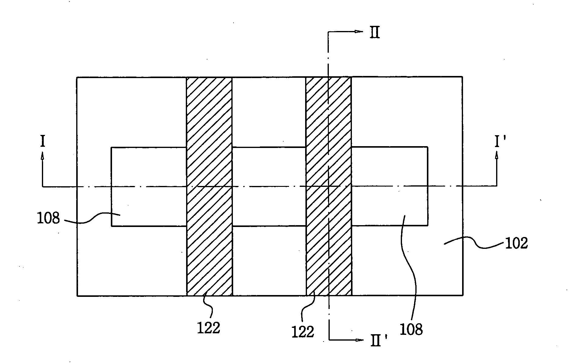
[0027]FIG. 1 illustrates a top view of a layout of a self-aligned recess channel transistor according to a first embodiment of the present invention. FIGS. 2 through 11 illustrate cross-sectional views of stages in a method of forming a self-aligned inner gate recess channel transistor according to the first embodiment of the present invention. More specifically, FIGS. 2 through 9 and 11 illustrate cross-sectional views taken along line I-I′ of FIG. 1 and FIG. 10 illustrates a cross-sectional view taken along line II-II′ of FIG. 1.

[0028]FIG. 1 illustrates a gate layer 122 formed over an active area 108 and a field area 102 of a semiconductor substrate. FIG. 1 includes cross-sectional lines I-I′ and II-II′ taken along an x-direction and a y-direction, respectively, of the semiconductor substrate.

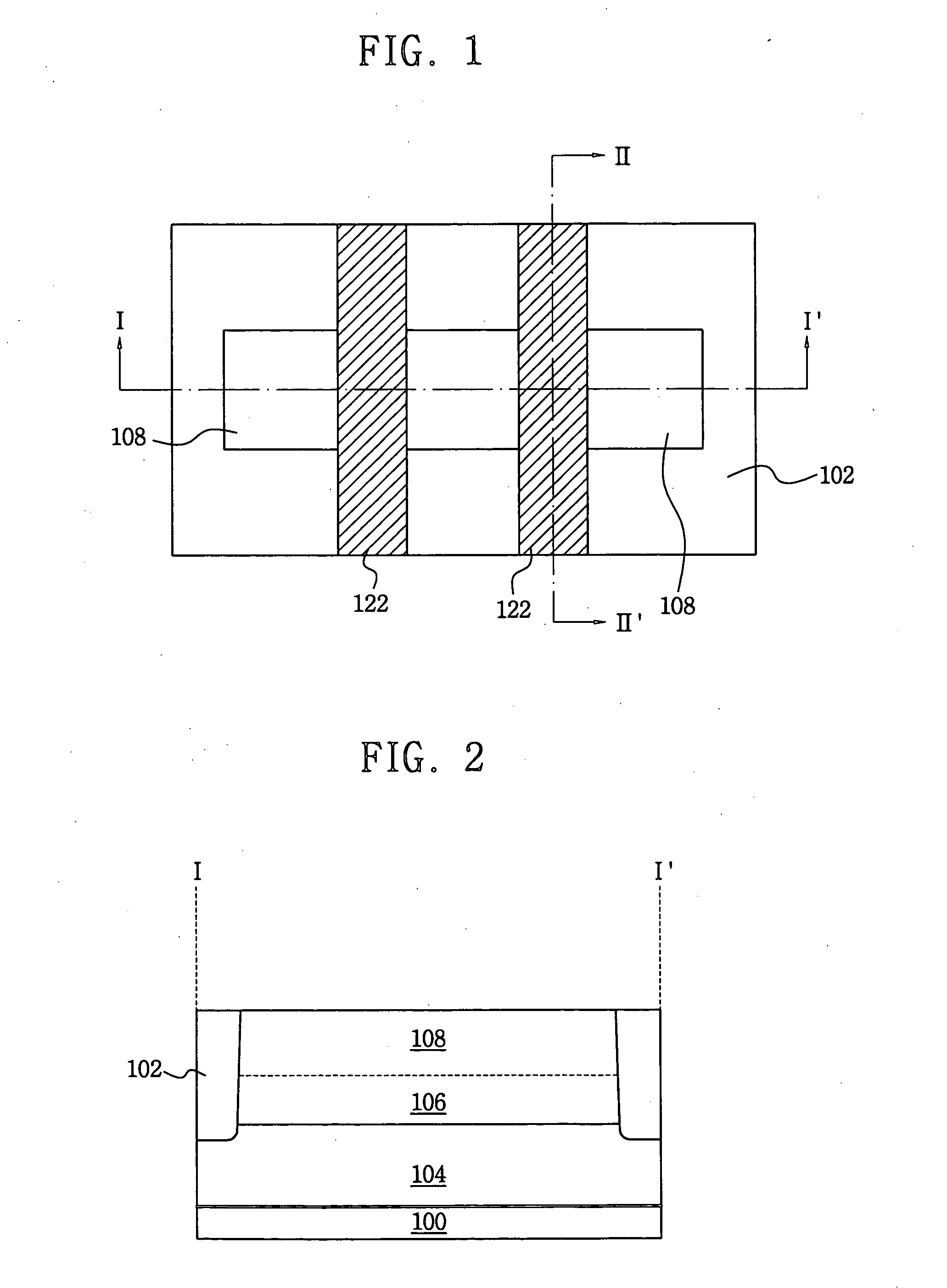
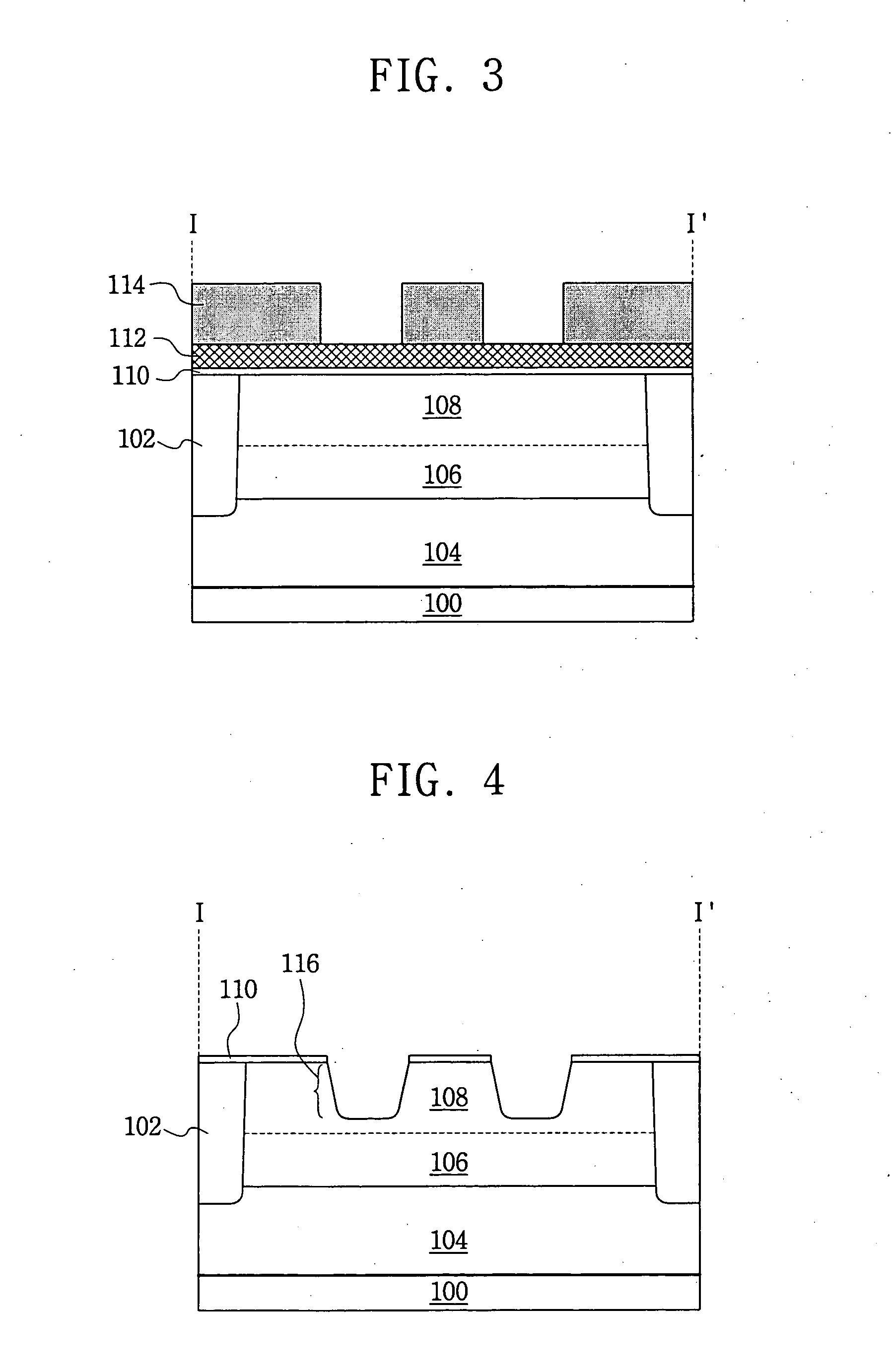
[0029] Referring now to FIG. 2, FIG. 2 illustrates a cross-sectional view, taken along line I-I′ of FIG. 1, of an initial stage in the method of forming the self-aligned inner gate recess c...

second embodiment

[0037]FIG. 12 illustrates a top view of a layout of a self-aligned recess channel transistor according to a second embodiment of the present invention. FIGS. 13 through 22 illustrate cross-sectional views of stages in a method of forming a self-aligned inner gate recess channel transistor according to the second embodiment of the present invention. More specifically, FIGS. 13 through 20 and 22 illustrate cross-sectional views taken along line I-I′ of FIG. 12 and FIG. 21 illustrates a cross-sectional view taken along line II-II′ of FIG. 12.

[0038]FIG. 12 illustrates a gate layer 222 formed over an active area 208 and a field area 202 of a semiconductor substrate. FIG. 12 includes cross-sectional lines I-I′ and II-II′ taken along an x-direction and a y-direction, respectively, of the semiconductor substrate.

[0039] Referring to FIG. 13, FIG. 13 illustrates a cross-sectional view, taken along line I-I′ of FIG. 12, of an initial stage in the method of forming the self-aligned inner gate...


PUM


Abstract

A self-aligned inner gate recess channel in a semiconductor substrate includes a recess trench formed in an active region of the substrate, a gate dielectric layer formed on a bottom portion of the recess trench, recess inner sidewall spacers formed on sidewalls of the recess trench, a gate formed in the recess trench so that an upper portion of the gate protrudes above an upper surface of the substrate, wherein a thickness of the recess inner sidewall spacers causes a center portion of the gate to have a smaller width than the protruding upper portion and a lower portion of the gate, a gate mask formed on the gate layer, gate sidewall spacers formed on the protruding upper portion of gate and the gate mask, and a source / drain region formed in the active region of the substrate adjacent the gate sidewall spacers.

Description

BACKGROUND OF THE INVENTION [0001] 1. Field of the Invention [0002] The present invention relates to a recess channel transistor and a method of forming the same. More particularly, the present invention relates to a self-aligned recess channel transistor having an inner gate with a center portion that has a smaller width than a protruding upper portion and a lower portion of the gate and a method of forming the same. [0003] 2. Description of the Related Art [0004] Conventionally, a recess transistor is used to achieve a higher density as a cell size is scaled down to the sub-micron range. As a planar gate size narrows in a recess transistor, however, short channel effects, junction leakage, and source / drain breakdown voltage become significant issues. Conventional recess gates have several disadvantages. A disadvantage of a conventional recess transistor, for example, is a large gate oxide area, which increases a gate loading capacitance. Additionally, another disadvantage of a con...

Claims


Application Information

Patent Timeline
Patent Type & Authority Applications(United States)
IPC IPC(8): H01L21/336H01L21/28H01L29/423H01L29/49H01L29/78
CPCH01L29/4238H01L29/7834H01L29/66621H01L29/66553H01L21/18
Inventor KIM, JI-YOUNGCHO, CHANG-HYUNSHIN, SOO-HOCHUNG, TAE-YOUNG
Owner SAMSUNG ELECTRONICS CO LTD
Features
  • Generate Ideas
  • Intellectual Property
  • Life Sciences
  • Materials
  • Tech Scout
  • Unparalleled Data Quality
  • Higher Quality Content
  • 60% Fewer Hallucinations
Learn More