
In-solid nuclear spin quantum calculation device

a quantum computation and solid-state technology, applied in the field of quantum processor devices, can solve problems such as the difficulty of spin control, the inability to solve the existing semiconductor technology, and the inability to control the nuclear spin at high speed

Inactive Publication Date: 2005-01-27
JAPAN SCI & TECH CORP
View PDF2 Cites 15 Cited by
  • Summary
  • Abstract
  • Description
  • Claims
  • Application Information

AI Technical Summary

Benefits of technology

According to the present invention, scattering of electron spins that is accompanied by their inversion between quantum Hall edge states realized in a two dimensional system in a semiconductor allows nuclear spins in a limited region to be inversed, thus to make a preparation of an initial state before a quantum bit is processed.
Also, according to the present invention, applying a bias voltage to the microfine radiofrequency waveguide mounted in a limited area in the vicinity of channel edges allows adjusting the NMR frequency for nuclear spins.

Problems solved by technology

The abovementioned theoretical proposal involves problems such as the need to completely remove impurities out of a silicon crystal, a technique of implanting precisely at a given location therein with a 31P ion and micromachining at a precision in the order of 0.05 micrometer, all of which appear to be impossible to solve by the existing semiconductor technologies.
This may cause the entire two dimensional electronic system, the electrodes and the lead wires to be heated and the quantum Hall effect to collapse, preventing the nuclear spin from being controlled at high speed.
The device has also the difficulty that the spin control has to be effected simultaneously for the nuclear spins existing in the entire two dimensional electronic system.
Thus, the prior in-solid nuclear spin quantum processor devices by theoretical proposals have been found either impossible to manufacture because of the need for a semiconductor microstructure that cannot be realized in the existing level of technologies or to fail to allow only a limited number of spins to be controlled and read out.

Method used


Image

  • In-solid nuclear spin quantum calculation device
  • In-solid nuclear spin quantum calculation device
  • In-solid nuclear spin quantum calculation device

Examples


Embodiment Construction

Hereinafter, the present invention will be described in detail with reference to certain suitable forms of implementation thereof illustrated in the drawing figures.

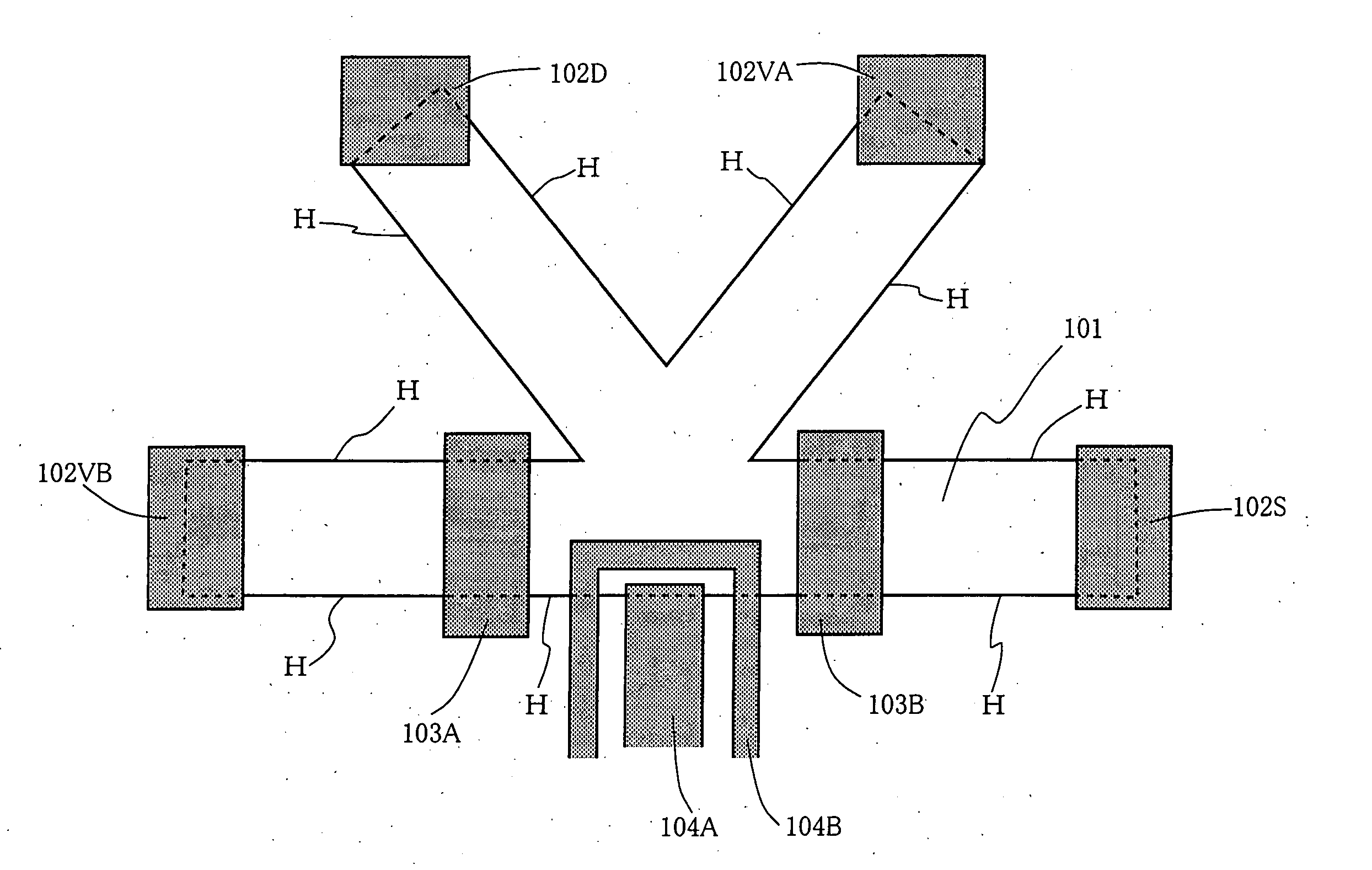
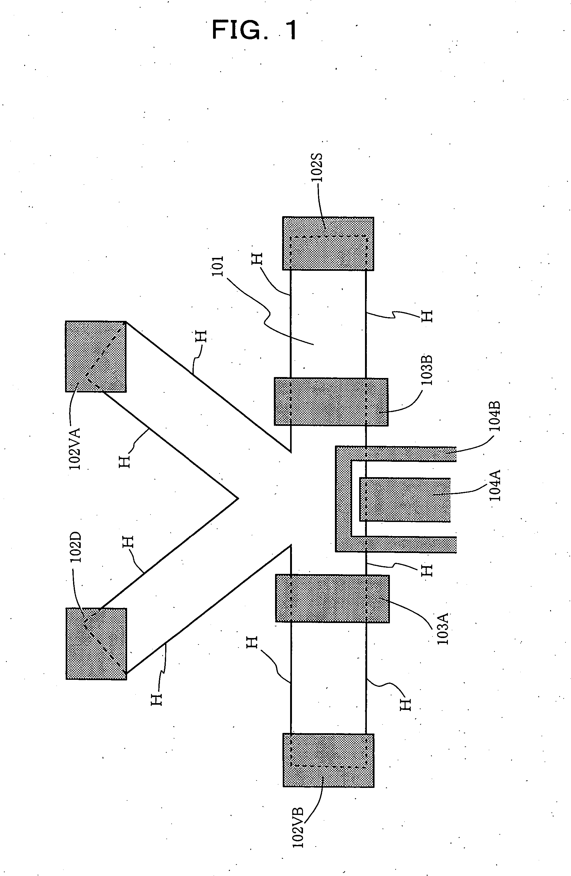
FIG. 1 is a plan view illustrating the makeup of a typical embodiment of the in-solid nuclear spin quantum processor device of the present invention.

In the Figure there are shown a two dimensional electronic system 101 using solid material, ohmic electrodes 102S, 102D, 102VA and 102VB made of metal, Schottky gate electrodes 103A and 103B made of metal, a waveguide comprising a core wire 104 made of metal and a ground wire 104B made of metal, which are coplanar.

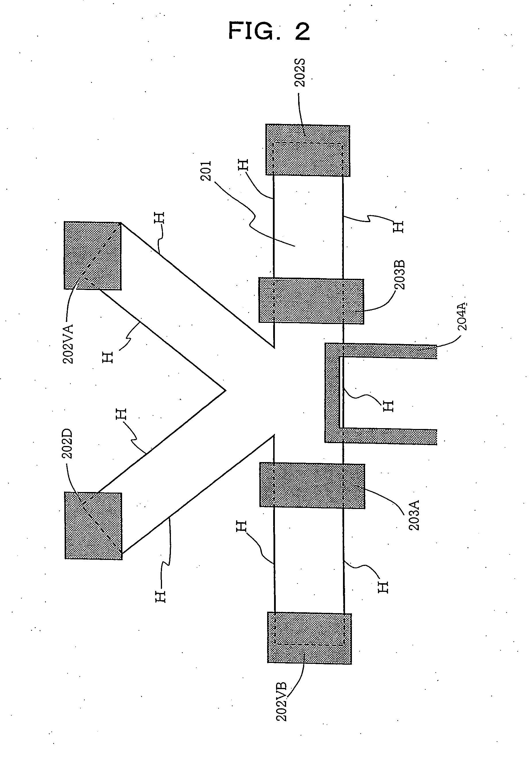
The makeup of another embodiment of the present invention is shown in FIG. 2. In the Figure there are shown a two dimensional electronic system 201 using solid material, ohmic electrodes 202S, 202D, 202VA and 202VB made of metal, Schottky gate electrodes 203A and 203B made of metal, and a microstrip waveguide 204A made of metal.

The two dimensional electroni...


PUM


Abstract

A voltage is applied across gate electrodes (103A) and (103B) in a two-dimensional electronic system (101) placed under a magnetic field, and the polarity of an electric current passed between ohmic electrodes (102D) and (102S) is selected to bring about inversion of electron spins based on a non-equilibrium distribution of electrons in a quantum Hall edge state and to initialize the polarization of nuclear spins. An oscillatory electric field of a nuclear magnetic resonance frequency is applied to coplanar waveguides (104A) and (104B) to control the nuclear spin polarization. The controlled spin polarization is read out by measuring the Hall resistance from ohmic electrodes (102VA) and (102VB). An in-solid nuclear spin quantum processor device can be manufactured by attaching a microfine metal gate structure to a quantized Hall effect element that is realized in a semiconductor two-dimensional system, and allows a limited number of nuclear spins to be controlled, initialized, subjected to a unitary transformation, and read out.

Description

TECHNICAL FIELD The present invention relates to a quantum processor device utilizing a nuclear spin system in solid for use in a quantum computer. BACKGROUND ART The quantum computer is a computer that is overwhelmingly high in the speed of computation in solving those specific problems which are virtually impossible to compute with classical computers. It uses units in a quantum two level system called quantum bits corresponding to bits used in the classical computer. While the quantum computer uses a large number of quantum bits in computation, it is basically operated by a quantum processor device that performs unitary transformation for any given quantum bit and reads out the quantum bit after the transformation. An explanation is given of basic particulars by taking a spin as an example. In general, applying a static magnetic field to a spin having a quantum number of 1 / 2 allows the spin to take one of two states that it is oriented parallel (upwards) and anti-parallel (dow...

Claims


Application Information

Patent Timeline
IPC IPC(8): G06N99/00H01L29/66
CPCB82Y10/00H01L29/66984G06N99/002G06N10/00
Inventor MACHIDA, TOMOKIKOMIYAMA, SUSUMUYAMAZAKI, TOMOYUKI
Owner JAPAN SCI & TECH CORP
Learn More