Semiconductor light-emitting device

a semiconductor and light-emitting device technology, applied in the direction of lasers, semiconductor lasers, printing, etc., can solve the problems of large scattering in the light-emitting properties of semiconductor light-emitting devices, interference may occur,

Active Publication Date: 2005-02-03
OKI ELECTRIC IND CO LTD
View PDF3 Cites 13 Cited by
  • Summary
  • Abstract
  • Description
  • Claims
  • Application Information

AI Technical Summary

Benefits of technology

It is therefore an object of the present invention to reduce the scatter in light-emitting properties of a semiconductor light-emitting device by setting the thickness of the semiconductor light-emitting device to a value at which interference between emitted light rays does not easily occur.
According to the present invention, the thickness of a semiconductor light-emitting thin film is set to a value at which interference between light rays extracted from a first surface of the semiconductor light-emitting thin film does not occur, i.e., the thickness of the semiconductor light-emitting thin film is set to a value at which the variations in light-emitting properties due to scatter in the thickness of the semiconductor light-emitting thin film are small, so the scatter in light-emitting properties between different semiconductor light-emitting devices or between plural light-emitting parts in the same semiconductor light-emitting device, can be reduced.

Problems solved by technology

However, if an optically reflecting surface (in Patent Reference 1, the light-reflecting film and the anode electrode) is formed on both surfaces of the semiconductor light-emitting layer, interference may occur due to the superimposition of the light rays generated in the active layer which pass through the main surface of the semiconductor light-emitting layer, and the light rays generated in the active layer which pass through the main surface of the semiconductor light-emitting layer after being reflected by the optically reflecting surfaces on both sides of the semiconductor light-emitting layer.
Under the conditions where such interference occurs, the spectral distribution largely varies due to scatter in the film thickness of the semiconductor light-emitting layer or the reflectivity of the optically reflecting surfaces, and therefore there is a large scatter in the light-emitting properties of the semiconductor light-emitting device due to manufacturing error.

Method used


Image

  • Semiconductor light-emitting device
  • Semiconductor light-emitting device
  • Semiconductor light-emitting device

Examples


first embodiment

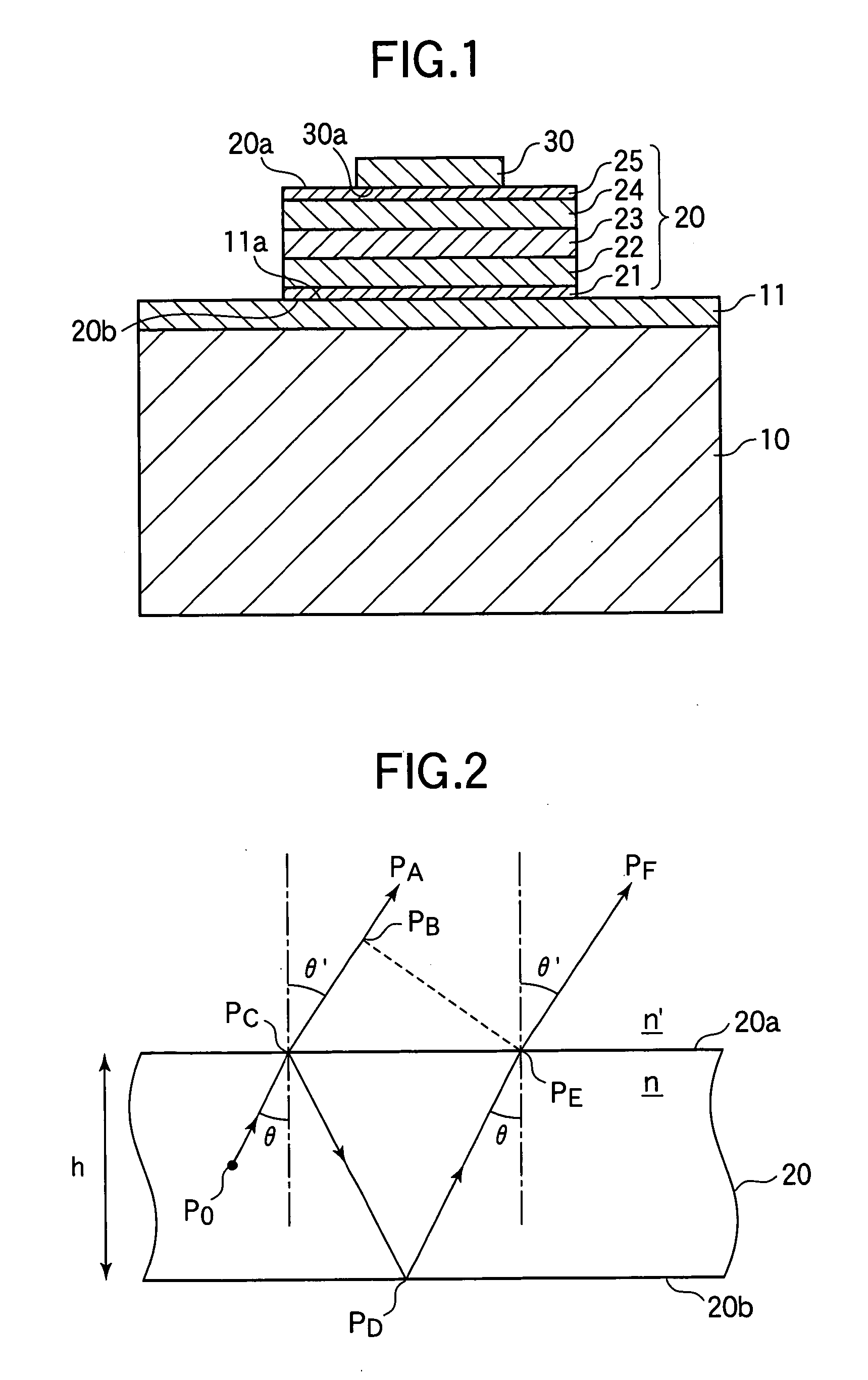
FIG. 1 is a cross-sectional view schematically showing the construction of a semiconductor light-emitting device according to a first embodiment of the present invention. As shown in FIG. 1, the semiconductor light-emitting device according to the first embodiment includes a support 10, a metal layer 11 provided on the support 10, an LED epitaxial film (also referred to as “LED epi-film”) 20 which is a semiconductor light-emitting thin film disposed on the metal layer 11, and an electrode 30 disposed on the LED epitaxial film 20.

The support 10 may, for example, include a dielectric such as glass, a semiconductor such as Si (silicon), or a conductor such as Al (aluminum). The thickness of the support 10 may be given a value, for example, within a range of 10 μm-18 μm. The metal layer 11 may be formed from an electrically conducting metal such as Al or the like. However, the metal layer 11 can also be formed from another electrically conducting material which can be ohmically connec...

second embodiment

FIG. 6 is a perspective view schematically showing the construction of a semiconductor light-emitting device according to a second embodiment of the present invention. FIG. 7 is a cross-sectional view schematically showing a section through a line S7-S7 in FIG. 6. In FIG. 6 and FIG. 7, identical symbols are assigned to identical or corresponding parts of the construction of FIG. 1.

As shown in FIG. 6 and FIG. 7, the semiconductor light-emitting device according to the second embodiment includes a support 10, a metal layer 11 provided on the support 10, plural LED epitaxial films 20 (in FIG. 6, four are shown but the invention is not limited to four) arranged in one row on the metal layer 11, an insulating film 26 disposed on the LED epitaxial film 20, and an electrode 30 connected on the LED epitaxial film 20 via a contact hole 26a formed in the insulating film 26. The electrode 30 is connected to an electrode pad 31 disposed on the insulating film 26. The semiconductor light-emitt...

third embodiment

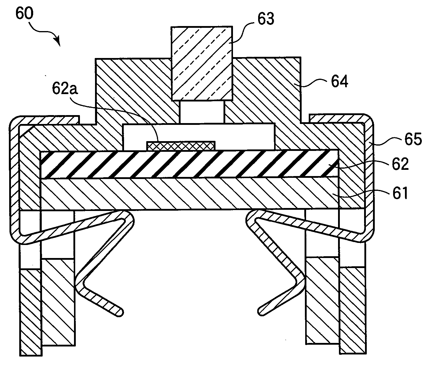
FIG. 8 is a cross-sectional view schematically showing the construction of an LED head according to a third embodiment of the present invention. As shown in FIG. 8, an LED head 60 includes a base member 61, an LED unit 62 fixed on the base member 61, a rod lens array 63 including pillar-shaped optical elements arranged in plural rows, a holder 64 which holds the rod lens array 63, and a clamp 65 which fixes these structures 61-64. The LED unit 62 includes an LED array chip (or LED / driving-IC chip) 62a. The LED array chip 62a includes one or more of the semiconductor light-emitting devices of the first or second embodiments arranged in plural rows. Light generated by the LED array chip 62a is emitted outside via the rod lens array 63. The LED head 60 is used as a light exposure device for forming an electrostatic latent image in an electrophotographic printer or an electrophotographic copier. The construction of the LED head including the semiconductor light-emitting device of the fi...


PUM


Abstract

A semiconductor light-emitting device includes a semiconductor light-emitting thin film, the thickness h of which satisfies the following conditional equation: 0.9×(2⁢m+1)⁢λ04⁢n≦h≦1.1×(2⁢m+1)⁢λ04⁢nand m in the conditional equation satisfies the following conditional equation: 2⁢m+1m⁡(m+1)⁢λ02>ξwhere λ0 is a center wavelength of light generated in the semiconductor light-emitting thin film, n is a refractive index of the semiconductor light-emitting thin film, m is 0 or a positive integer, and ξ is a half bandwidth of a light emission spectrum when there is no interference between light rays generated in the semiconductor light-emitting thin film.

Description

BACKGROUND OF THE INVENTION 1. Field of the Invention The present invention relates to a surface light-emitting type semiconductor light-emitting device such a double hetero LED or a laser, to an LED head including the semiconductor light-emitting device, to an image-forming apparatus including the semiconductor light-emitting device, and to a method of manufacturing the semiconductor light-emitting device. 2. Description of the Related Art A semiconductor light-emitting device wherein a light-reflecting film, semiconductor light-emitting layer and anode electrode are laminated successively on an electrically conducting plate (cathode electrode) has been proposed in, for example, Japanese Patent Application Laid-Open Publication No. 2002-217450 (pp. 5-7, FIG. 1), which is referred to “Patent Reference 1.” This semiconductor light-emitting device has a surface light-emitting construction wherein light which has been generated in an active layer of the semiconductor light-emitting...

Claims


Application Information

Patent Timeline
Patent Type & Authority Applications(United States)
IPC IPC(8): B41J2/45H01L29/06H01L33/00H01L33/08H01L33/30H01L33/58H01S5/10H01S5/183
CPCB41J2/45H01L33/465H01L33/405
Inventor FUJIWARA, HIROYUKIOGIHARA, MITSUHIKO
Owner OKI ELECTRIC IND CO LTD
Why Eureka
Try Eureka