Delay circuit and delay sysnchronization loop device

Inactive Publication Date: 2005-02-03
LONGITUDE SEMICON S A R L
View PDF8 Cites 71 Cited by
  • Summary
  • Abstract
  • Description
  • Claims
  • Application Information

AI Technical Summary

Benefits of technology

[0018] Accordingly, it is an object of the present invention to provide a simplified delay circuit, generating different propagation time for the signal rise

Problems solved by technology

However, in the conventional coarse delay line CDL, shown in FIGS. 21 and 23, it is not possible to set the rise or

Method used


Image

  • Delay circuit and delay sysnchronization loop device
  • Delay circuit and delay sysnchronization loop device
  • Delay circuit and delay sysnchronization loop device

Examples


Example

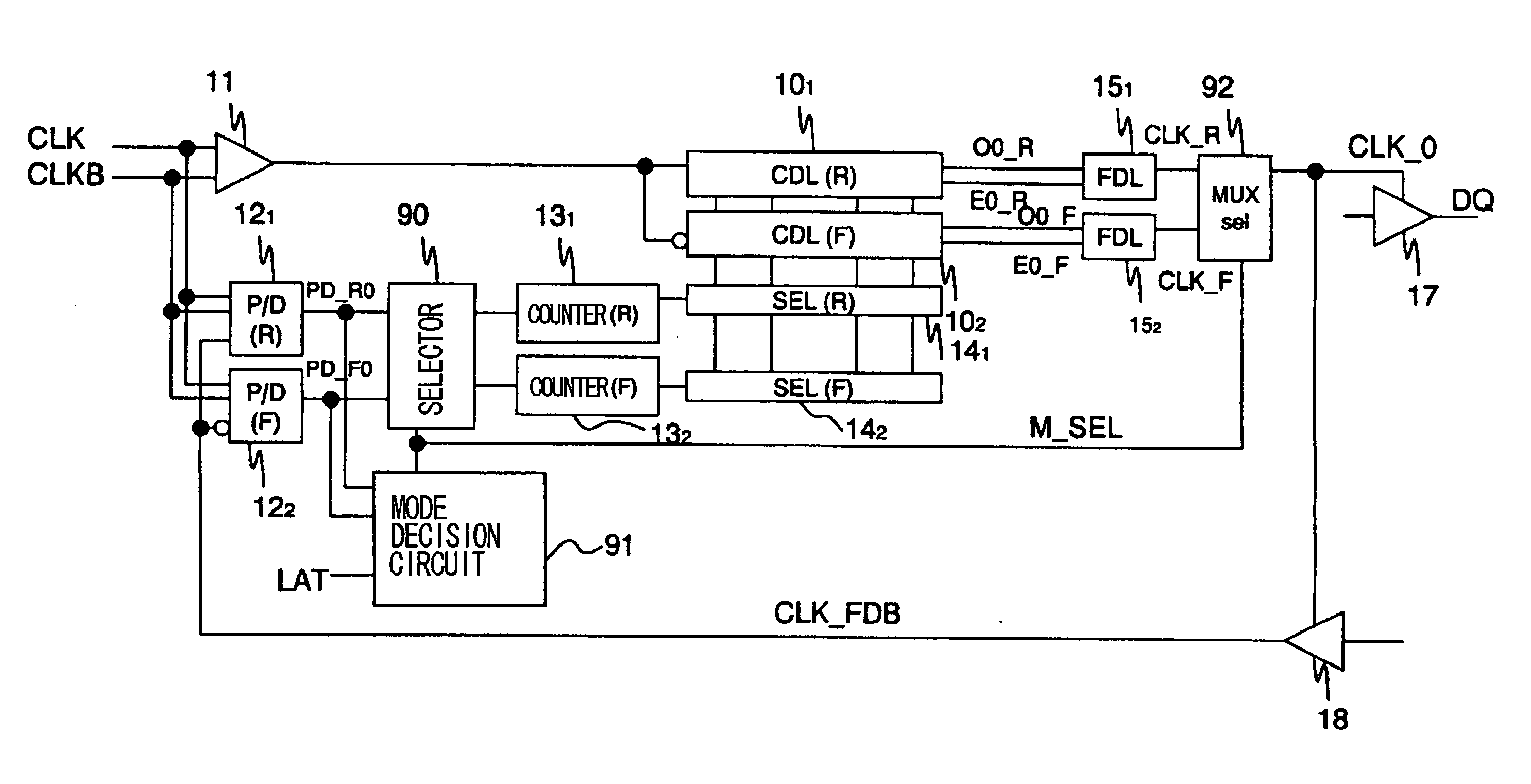
[0059] The preferred mode for carrying out the present invention is now explained. The present invention comprises a delay line circuit in which the propagation path for the rising edge and that for the falling edge of an input signal are independently selected to provide for a variable duty ratio. By this delay line circuit, the DLL of, for example, x.5 mode (1.5T mode if x=1) may be realized.

[0060] That is, if a mode (1.5T mode) in which a data output DQ by the delay from the rising edge (CLK↑) is synchronized with the fall of the clock signal (CLK↓) (see “Rise propagation”) and the delay of the data output DQ by the delay from the falling edge (CLK↓) is synchronized with the rise of the clock signal (CLK↑) (see “Fall propagation”), as shown in FIG. 3C, can be set, the (maximum) propagation time may be shortened to diminish the jitter.

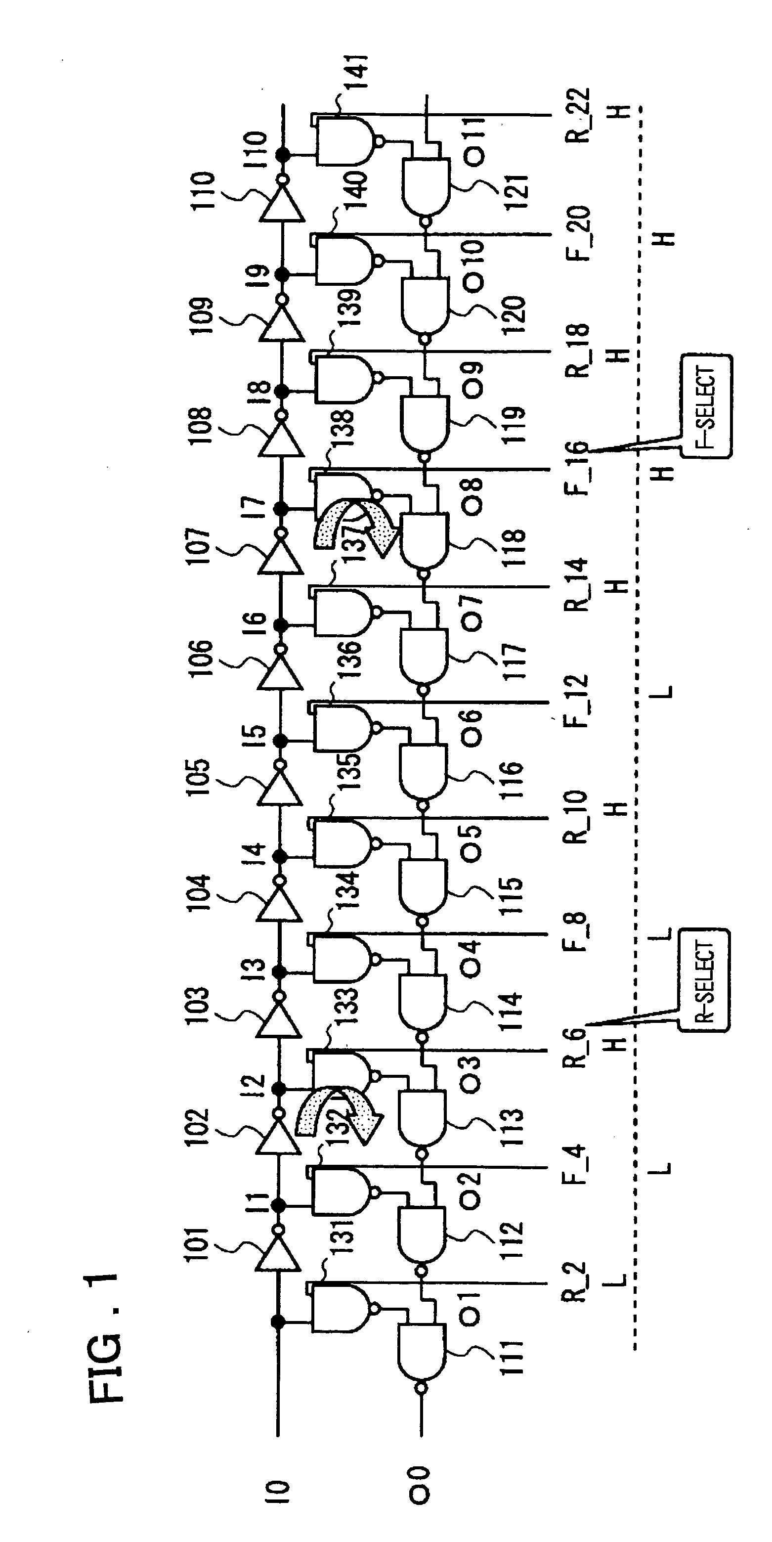
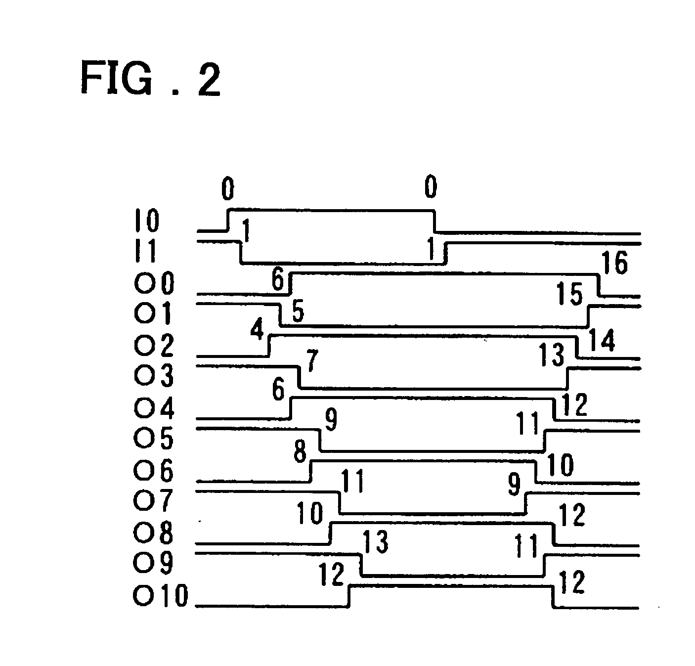
[0061] More specifically, a delay circuit according to a preferred embodiment of the present invention includes a first delay line circuit having ...


PUM


Abstract

A delay circuit includes a first delay line circuit having a plurality of stages of delay units, a second delay line circuit having a plurality of stages of delay units, a plurality of transfer circuits provided in association with respective stages of the delay units of the first delay line circuit, the transfer circuits controlling the transfer of the outputs of the delay units of the first delay line circuit to associated stages of the delay units of the second delay line circuit. The delay units of respective stages of the first delay line circuit inverting input signals. Each stage delay unit of the second delay line circuit includes a logic circuit receiving an output signal of the transfer circuit associated with the delay unit in question and an output signal of a preceding stage to send an output signal to a following stage. The duty ratio is rendered variable by independently selecting the rising edge of the input signal and a propagation path of the falling edge.

Description

FIELD OF THE INVENTION [0001] This invention relates to a delay circuit and, more particularly, to a delay circuit preferably applied to a delay locked loop (DLL). BACKGROUND OF THE INVENTION [0002]FIG. 21 schematically shows an illustrative structure of a DLL (delay lock loop) used e.g. in a conventional DDRII / I-SDRAM (Double Delta Rate II-Synchronous DRAM). Referring to FIG. 21, the DLL is made up by two control circuits and two coarse delay lines CDL 10 having a variable delay time. The control circuit is composed of a phase detector (P / D) 12, also termed a phase comparator, and a counter 13. An output of a receiver 11, which receives complementary clock signals CLK and CLKB, is supplied to the coarse delay line CDL 10, output pairs O0 and E0 of which are supplied to a fine delay line FDL 15, composed of a phase interpolator, for phase adjustment. A multiplexer 17 receives output data signals, not shown, in parallel, and selects and outputs the output data signal to a data termin...

Claims


Application Information

Patent Timeline
IPC IPC(8): G06F1/10G11C11/407G11C11/4076H03K5/04H03K5/13H03L7/081H03L7/087
CPCH03K5/133H03K5/135H03K2005/00058H03L7/087H03K2005/00247H03K2005/00273H03L7/0814H03K2005/00241H03L7/0818
Inventor TAKAI, YASUHIROKOBAYASHI, SHOTARO
Owner LONGITUDE SEMICON S A R L
Why Eureka
Try Eureka