Electrode manufacturing method

a manufacturing method and technology of electrodes, applied in the manufacture of electrode systems, electric discharge tubes/lamps, instruments, etc., can solve the problems of inability to form gate electrodes and drain electrodes with respect to each carbon nanotube arranged in a matrix array at intervals less than several tens of nanometers, and the inability to form source electrodes and drain electrodes with respect to each carbon nanotub

Inactive Publication Date: 2005-02-03
KK TOSHIBA
View PDF9 Cites 34 Cited by
  • Summary
  • Abstract
  • Description
  • Claims
  • Application Information

AI Technical Summary

Benefits of technology

An advantage of an aspect of the present invention is to provide an electrode manufacturing method for enabling formation of an electrode to a microstructure such as a carbon nanotube or quantum dot in a self-alignment manner in order to solve the above described problems.

Problems solved by technology

However, in a conventional lithography technology, it has been impossible to form electrodes in such microstructures with an accuracy less than several nanometers.
For example, it has been impossible to form gate electrodes and drain electrodes with respect to each carbon nanotube arranged in a matrix array at intervals less than several tens of nanometers.
Further, in the non-patent document 3, a transistor using a carbon nanotube is disclosed, however, by the technology disclosed in the document, source electrodes and drain electrodes can not be formed with respect to each carbon nanotube.
This is a disadvantage in light of high integration of the transistor.
This is a disadvantage in high integration of the field emitter and miniaturization of the FED.
However, conventionally, it has been impossible to provide electrodes to such quantum dots, respectively.

Method used


Image

  • Electrode manufacturing method
  • Electrode manufacturing method
  • Electrode manufacturing method

Examples


second embodiment

(Second Embodiment)

FIGS. 5 to 14 show processes of forming a single electron transistor element according to the second embodiment of the invention in the order of the processes. FIGS. 5, 6, 8, 9, and 12 show the structure on a silicon substrate 10 in sectional views. FIGS. 7, 10, 11, 13, and 14 show the structure on the silicon substrate 10 in plan views.

Referring to FIG. 5, first, a silicon oxide film 20 is formed on the silicon substrate 10 by oxidizing the silicon substrate 10. Then, an aluminum layer 21 having a thickness of about 10 nm is deposited on the silicon oxide film 20. An Al2O3 layer 23 having a thickness of about 1 nm is formed on the aluminum layer 21 by natural oxidization of the aluminum layer 21.

Next, an aluminum layer 25 having a thickness of about 2 nm is deposited on the Al2O3 layer 23. An Al2O3 layer 27 having a thickness of about 1 nm is formed on the aluminum layer 25 by natural oxidization of the aluminum layer 25. Further, an aluminum layer 29 having...

third embodiment

(Third Embodiment)

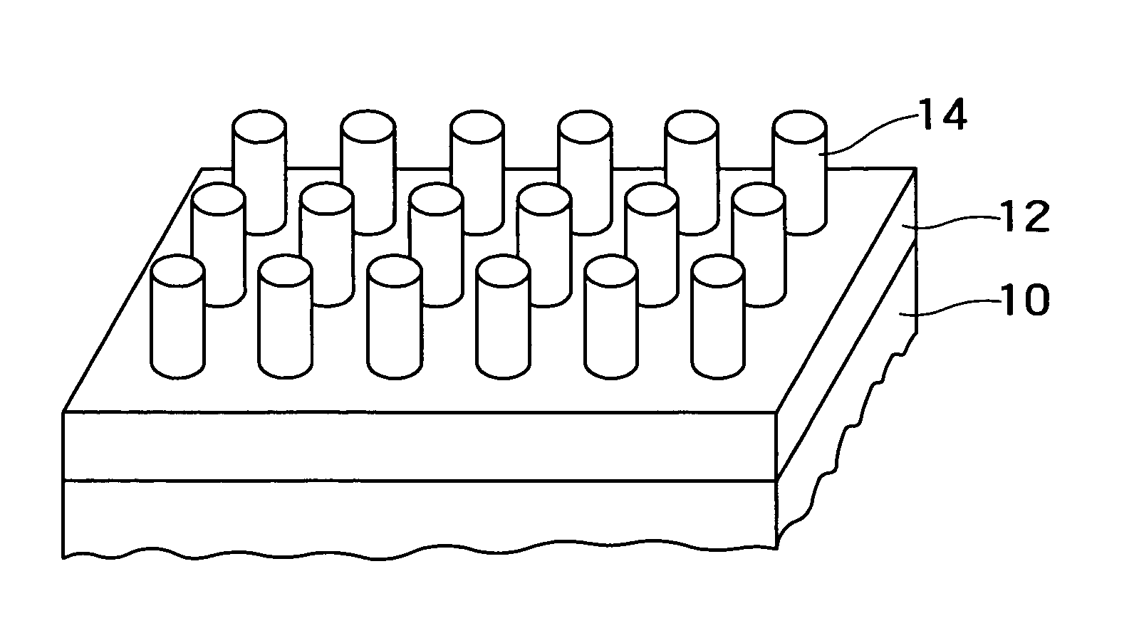
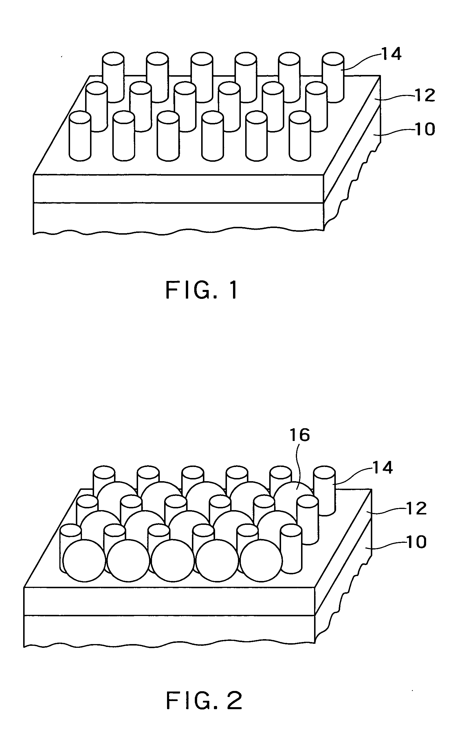
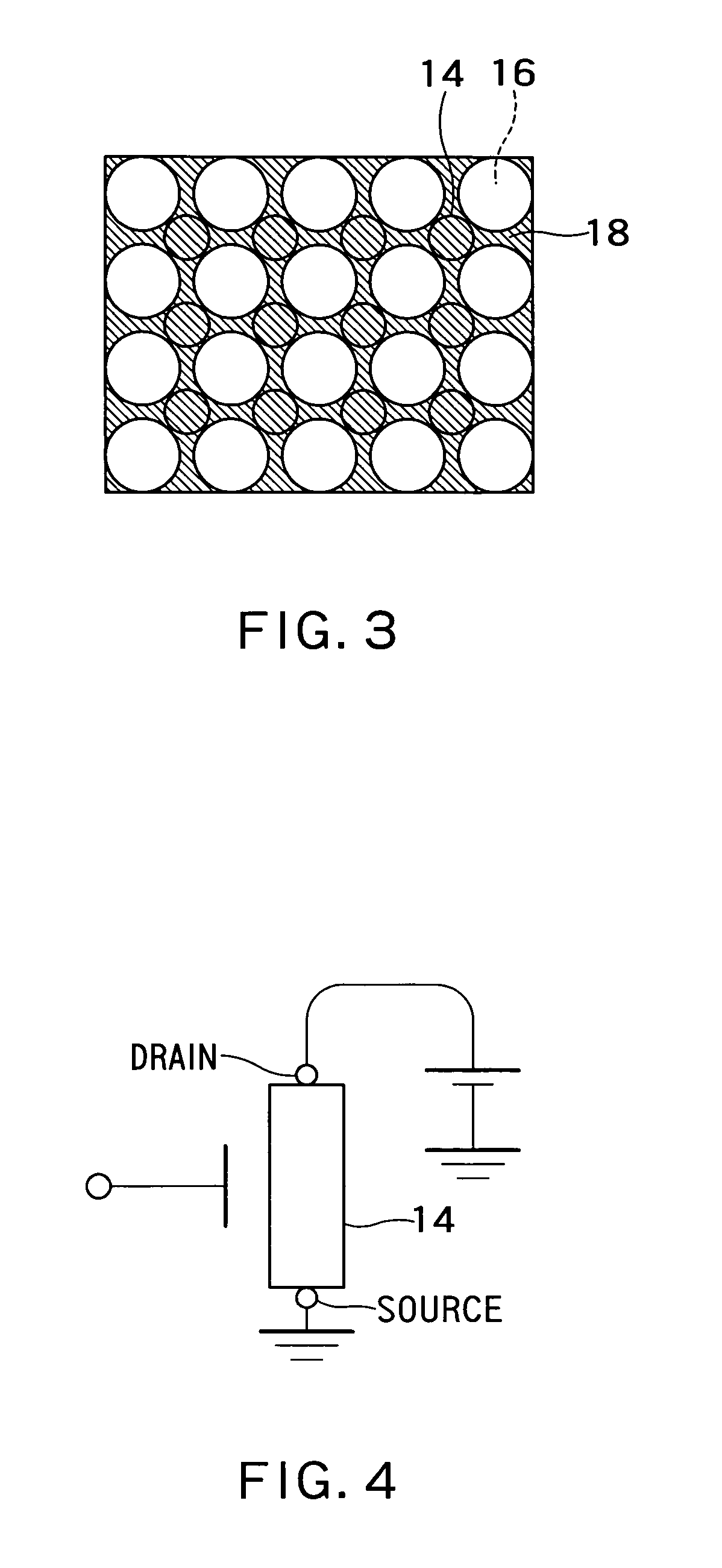
FIGS. 15 to 17 are sectional views showing manufacturing processes of a field emitter according to the third embodiment of the invention in the order of the processes. Referring to FIG. 15, first, carbon nanotubes 51 are arranged in a matrix form on a substrate 50. The carbon nanotubes 51 are formed by the method disclosed in the non-patent document 2.

Then, polystyrene derivatives 53 are applied onto the substrate 50. At this time, the polystyrene derivatives 53 are included in a solvent, and applied by the spin casting method. When the solvent is volatilized, the polystyrene derivatives 53 are arranged between the carbon nanotubes 51. At that time, the size of the polystyrene derivative 53 may be changed in the same manner as in the first embodiment. The polystyrene derivatives 53 are designed so as to have top portions higher than the tip ends of the carbon nanotubes 51 when arranged between the carbon nanotubes 51. Alternatively, by stacking plural of the pol...

fourth embodiment

(Fourth Embodiment)

FIGS. 18 to 24 are sectional views showing manufacturing processes of a quantum bit (qubit) according to the fourth embodiment of the invention in the order of the processes. FIGS. 18 to 20 show the structure on a silicon substrate 10 in sectional views. FIGS. 21 to 24 show the structure on the silicon substrate 10 in plan views. The embodiment is a method for manufacturing an electrode on a quantum bit formed by electrically bonding two quantum dots, which is disclosed in the non-patent document 5.

Referring to FIG. 18, first, an element area is formed on the surface of the silicon substrate 10, and a silicon oxide film 70 having a thickness of about 7 nm is formed on the surface of the silicon substrate 10. Then, a polysilicon layer 71 having a thickness of about 5 nm is deposited on the silicon oxide film 70 by the CVD method or the like. A silicon oxide film 73 is formed on the polysilicon layer 71 by the CVD method or the like. A polysilicon layer 75 having...


PUM

PropertyMeasurementUnit
capacitanceaaaaaaaaaa
heightaaaaaaaaaa
sizeaaaaaaaaaa

Abstract

An electrode manufacturing method comprises: forming plural protruding portions on a surface of a substrate; introducing first particles having a size that changes according to heat, light, or a first solvent between said plural protruding portions; changing the size of the first particles by applying heat, light, or the first solvent to said first particles; and depositing an electrode material onto the surface of said substrate.

Description

CROSS-REFERENCE TO RELATED APPLICATION This application is based upon and claims the benefit of priority from the prior Japanese Patent Application No. 2003-285347, filed on Aug. 1, 2003, the entire contents of which are incorporated herein by reference. BACKGROUND OF THE INVENTION 1. Field of the Invention The present invention relates to an electrode manufacturing method. 2. Related Background Art Recently, a technology for manufacturing a microstructure equal to or less than several tens of nanometers such as a carbon nanotube and a quantum dot on a semiconductor substrate has been developed. For example, B. Q. Wei et al., Nature, Vol. 416, P495 (2002) (hereinafter, referred to as “Non-patent document 1”) discloses a technology for arraying carbon nanotubes on silicon oxide. Ago et al., Appl. Phys. Lett. Vol. 77, P79 (2000) (hereinafter, referred to as “Non-patent document 2”) discloses a technology for manufacturing a carbon nanotube using the CVD method. The carbon tubes d...

Claims


Application Information

Patent Timeline
Patent Type & Authority Applications(United States)
IPC IPC(8): B82B3/00C01B31/02H01J9/02H01L21/28H01L21/302H01L21/44H01L21/60H01L29/06H01L29/41H01L29/417H01L29/66H01L29/786H01L35/24
CPCB82Y10/00G11C13/025H01J9/025H01L29/0665Y10T428/259H01L29/0676H01L29/068Y10T428/256H01L29/0673
Inventor TANAMOTO, TETSUFUMISAITO, SATOSHIFUJITA, SHINOBU
Owner KK TOSHIBA
Why Eureka
Try Eureka