Substrate processing apparatus and substrate processing method

a substrate processing and substrate technology, applied in the direction of electrical equipment, semiconductor/solid-state device manufacturing, basic electric elements, etc., can solve the problems of contamination of the processing environment in other processes, inability to prevent water marks, and large number of water marks, so as to suppress the formation of water marks and increase the rotational speed of the substrate. , the effect of increasing the rotational speed of the substra

a substrate processing and substrate technology, applied in the direction of electrical equipment, semiconductor/solid-state device manufacturing, basic electric elements, etc., can solve the problems of contamination of the processing environment in other processes, inability to prevent water marks, and large number of water marks, so as to suppress the formation of water marks and increase the rotational speed of the substrate. , the effect of increasing the rotational speed of the substra

US20050026455A1Inactive Publication Date: 2005-02-03EBARA CORP

Image

  • Substrate processing apparatus and substrate processing method
  • Substrate processing apparatus and substrate processing method
  • Substrate processing apparatus and substrate processing method

Examples


Embodiment Construction

Embodiments of the present invention will hereinafter be described with reference to the drawings.

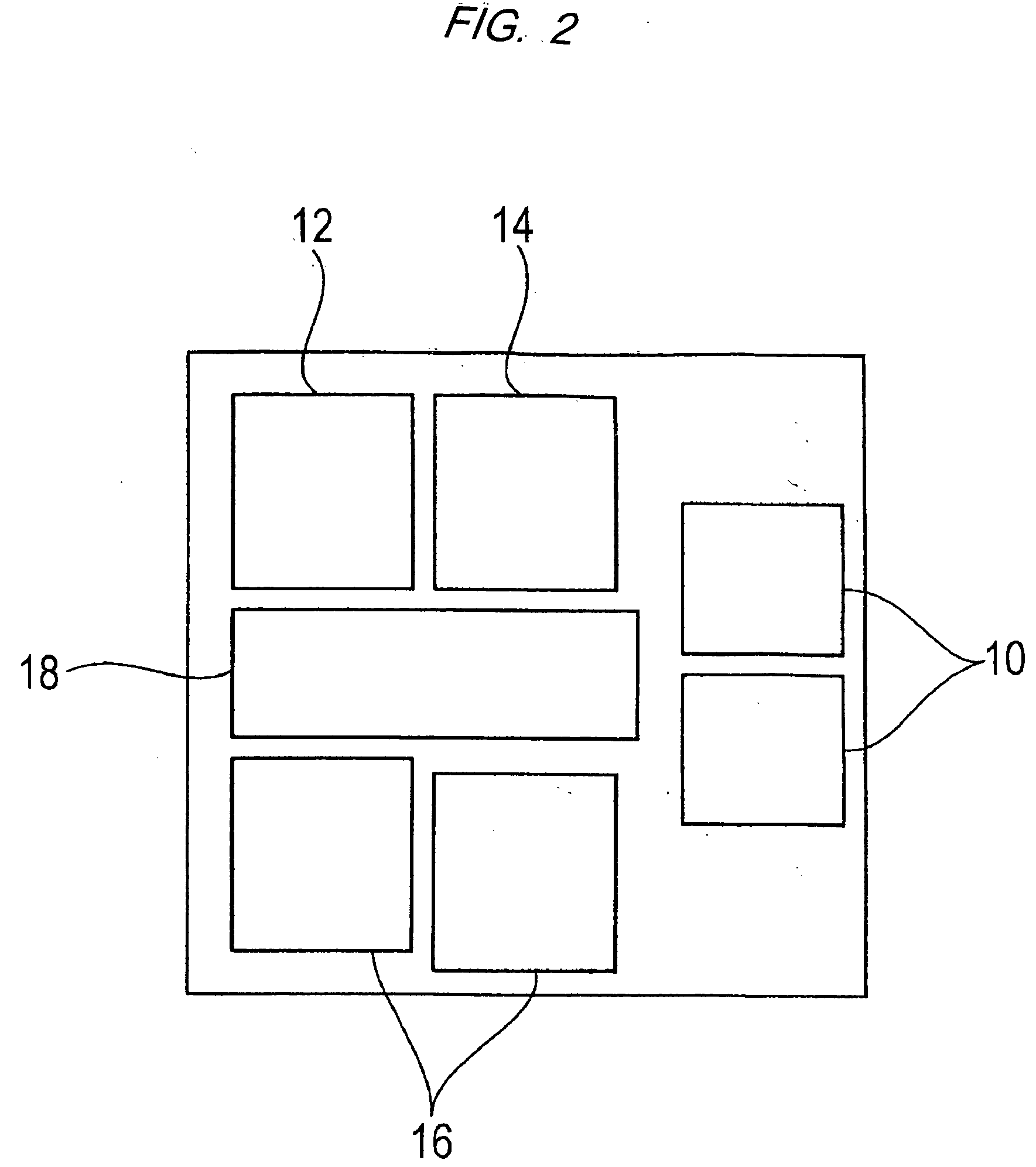
FIG. 2 is a view showing a planar layout of a substrate processing apparatus (system) according to an embodiment of the present invention. As shown in FIG. 2, the substrate processing system comprises two loading / unloading units 10 for placing thereon substrate cassettes housing substrates which each have a thin film deposited on its surface by, for example, sputtering, CVD, or plating, a polishing apparatus 12 for polishing away an unnecessary thin film deposited on or adhering to a bevel or edge portion of a substrate on which a thin film is formed, an etching apparatus 14 for etching away a thin film that remains on the bevel or edge portion of the substrate polished by the polishing apparatus 12, and cleaning / drying apparatuses 16 for cleaning and drying the substrate where the thin film on the bevel or edge portion thereof has been etched away by the etching apparatus 14. The sub...


PUM

PropertyMeasurementUnit
temperatureaaaaaaaaaa
humidityaaaaaaaaaa
diameteraaaaaaaaaa

Abstract

The present invention provides a substrate processing apparatus having a drying mechanism for removing water from the surface of a substrate which has been cleaned by a wet cleaning process, and a substrate processing apparatus and a substrate processing method which are capable of efficiently removing an unnecessary thin film deposited on or adhering to a bevel or edge portion of a substrate. The substrate processing apparatus of this invention has a substrate holder for holding a substrate, and a dry gas supply section for turning an atmosphere to which at least a portion of a surface of the substrate held by the substrate holder is exposed into a humidity-controlled dry gas atmosphere.

Description

BACKGROUND OF THE INVENTION 1. Field of the Invention The present invention relates to a substrate processing apparatus and a substrate processing method, and more particularly to a substrate processing apparatus having a drying mechanism for removing water from a surface of a substrate which has been cleaned by a wet cleaning process, and a substrate processing apparatus and a substrate processing method which are capable of efficiently removing an unnecessary thin film deposited on or adhering to a bevel or edge portion of a substrate. The present invention is also concerned with a substrate processing apparatus and a substrate processing method which can suppress the formation of water marks on a substrate. 2. Description of the Related Art In each of processing processes performed for the fabrication of semiconductor devices, it is widely practiced to process a substrate such as a semiconductor wafer or the like, and thereafter clean the substrate in a wet cleaning process ...

Claims


Application Information

Patent Timeline
03 Feb 2005
Publication
US20050026455A1
IPC
C23F1/18; H01L21/00; H01L21/02; H01L21/288; H01L21/306; H01L21/321; H01L21/3213
CPC
C23F1/18; H01L21/02074; H01L21/02087; H01L21/67051; H01L21/3212; H01L21/32134; H01L21/67028; H01L21/2885
Inventors
HAMADA, SATOMI; KONO, MICHIHISA