Multi-chip module
- Summary
- Abstract
- Description
- Claims
- Application Information
AI Technical Summary
Benefits of technology
Problems solved by technology
Method used
Image

Examples
Embodiment Construction
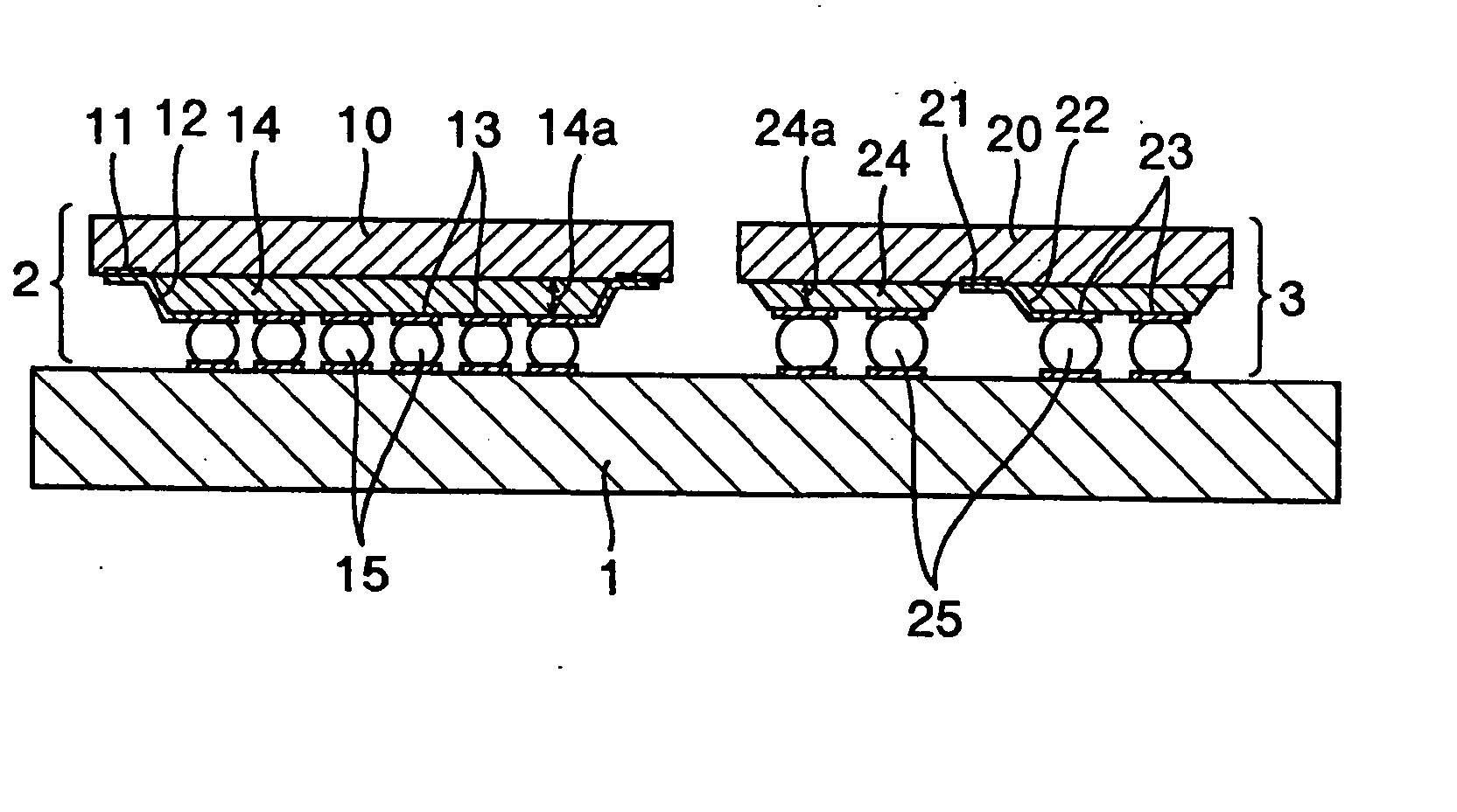
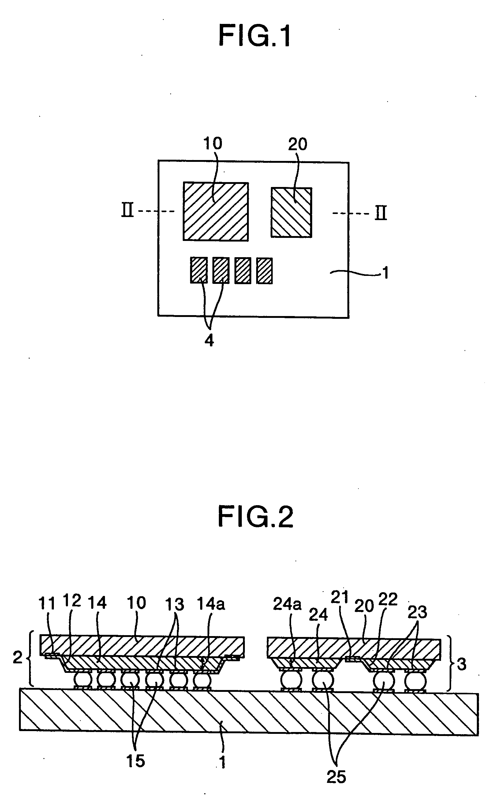
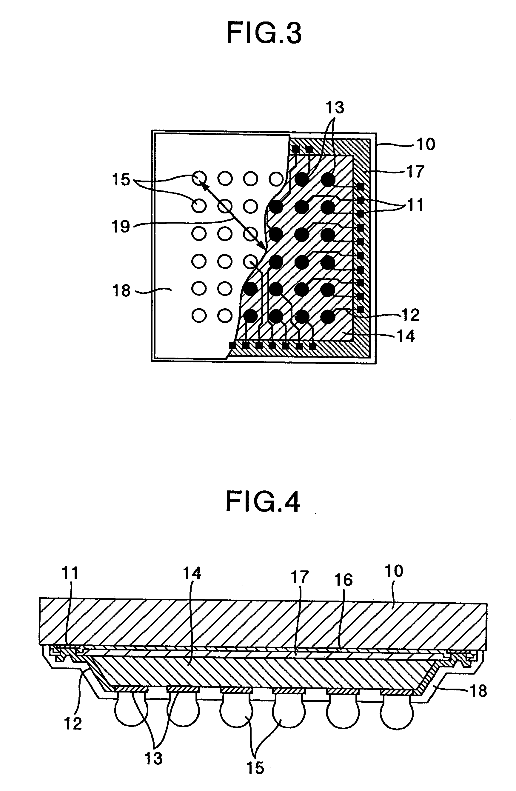
[0031] The invention is adaptable to a multi-chip module having a plurality of semiconductor devices and passive electronic components densely mounted on a board, and performing a function operable as one system. As such semiconductor devices to be mounted on the mounting board, for example, a CPU, microprocessor, logic, memory (DRAM, SRAM, Flash, etc.), or image-processing-dedicated chip, and a specific chip integrating interfaces or the like into a single chip, are variously considered depending on products. The passive components are chip-capacitors and / or resistors, which are assembled for stabilization of the circuit, such as for reducing noise. The components may be mounted inside of the mounting board.
[0032]FIGS. 1 and 2 are a plan view and a cross-sectional view of a first embodiment of the invention. As shown in FIG. 1, the first embodiment of the invention provides an example of a basic configuration, in which two semiconductor devices of a first semiconductor chip 10 and...
PUM
 Abstract
Description
Claims
Application Information
 - Generate Ideas
- Intellectual Property
- Life Sciences
- Materials
- Tech Scout
- Unparalleled Data Quality
- Higher Quality Content
- 60% Fewer Hallucinations
Browse by: Latest US Patents, China's latest patents, Technical Efficacy Thesaurus, Application Domain, Technology Topic, Popular Technical Reports.
© 2025 PatSnap. All rights reserved.Legal|Privacy policy|Modern Slavery Act Transparency Statement|Sitemap|About US| Contact US: help@patsnap.com